Podcast
Questions and Answers
What is the primary material used in wafer preparation for Integrated Circuits?
What is the primary material used in wafer preparation for Integrated Circuits?
- Gallium Arsenide
- Selenium
- Germanium
- Silicon (correct)
What is the main characteristic of monocrystalline silicon?
What is the main characteristic of monocrystalline silicon?
- It is less efficient than polycrystalline silicon.
- Its crystal lattice is continuous and unbroken. (correct)
- It contains multiple grain boundaries.
- It has a lower melting point than polycrystalline silicon.
Which of the following is NOT a subprocess of wafer preparation?
Which of the following is NOT a subprocess of wafer preparation?
- Wafer Final Polish
- Vacuum Deposition (correct)
- Wafer Scrubbing
- Wafer Slicing
Which method is specifically used to obtain monocrystalline semiconductors?
Which method is specifically used to obtain monocrystalline semiconductors?
What is the purpose of zone refining in wafer preparation?
What is the purpose of zone refining in wafer preparation?
How does polycrystalline silicon differ from monocrystalline silicon?
How does polycrystalline silicon differ from monocrystalline silicon?
What is the first step in the IC manufacturing process?
What is the first step in the IC manufacturing process?
Who discovered the Czochralski Pulling Technique?
Who discovered the Czochralski Pulling Technique?
What is the main material prepared for Integrated Circuit?
What is the main material prepared for Integrated Circuit?
Which of the following is NOT a subprocess of wafer preparation?
Which of the following is NOT a subprocess of wafer preparation?
Monocrystalline silicon has grain boundaries.
Monocrystalline silicon has grain boundaries.
What technique is used to obtain monocrystalline semiconductors?
What technique is used to obtain monocrystalline semiconductors?
What indicates that a wafer is free from contaminants after final polishing?
What indicates that a wafer is free from contaminants after final polishing?
Zone refining is also known as __________.
Zone refining is also known as __________.
What is the second most abundant element on earth?
What is the second most abundant element on earth?
Flashcards are hidden until you start studying
Study Notes
Integrated Circuits Overview
- Integrated Circuits (IC) consist of a collection of electronic components and their wiring, compacted onto a tiny slice of monocrystalline semiconductor material.
- Silicon, the primary material used for ICs, ranks as the second most abundant element on Earth, following Oxygen.
IC Manufacturing Process Stages
- The IC manufacturing process includes:
- Wafer Preparation
- Wafer Fabrication
- Wafer Sort
- Integrated Circuit Assembly
- Final Test
Wafer Preparation
- Wafer preparation is fundamental for IC production, focusing on silicon wafers as the main material.
Types of Silicon Crystals
- Monocrystalline Silicon:
- Characterized by a continuous and unbroken crystal lattice with no grain boundaries.
- Polycrystalline Silicon:
- Exhibits a more disordered structure, opposite the monocrystalline characteristics.
Subprocesses of Wafer Preparation
- Key subprocesses involve:
- Zone Refining
- Czochralski Pulling Technique
- Ingot Surface Grinding
- Ingot Slicing
- Wafer Scrubbing
- Wafer Rinsing
- Wafer Final Polish
- Resistivity Check and Inspection
Zone Refining
- Also known as zone melting or floating zone process, this technique allows for the purification of silicon.
- A narrow molten zone is moved along the crystal, melting impure solids at its leading edge and leaving behind purer material as it solidifies.
Czochralski Pulling Technique
- A crystal growth method used to produce monocrystalline semiconductors.
- Named after Jan Czochralski, who discovered this process in 1916 during experiments on the crystallization rates of metals.
Integrated Circuit Overview
- Integrated Circuit (IC) consists of electronic components and interconnections etched onto a small slice of monocrystalline semiconducting material.
- Silicon is the primary material for ICs and is the second most abundant element on Earth after oxygen.
IC Manufacturing Process
- Wafer Preparation is the first step, followed by Wafer Fabrication, Wafersort, Integrated Circuit Assembly, and Final Test.
Wafer Preparation
- Focuses on preparing silicon wafers.
- Essential sub-processes include:
- Zone Refining
- Czochralski Pulling Technique
- Ingot Surface Grinding
- Ingot Slicing
- Wafer Scrubbing
- Wafer Rinsing
- Wafer Final Polish
- Resistivity Check and Inspection
Types of Crystals
- Monocrystalline:
- Continuous crystal lattice without grain boundaries.
- Polycrystalline:
- Comprises multiple grains, contrasting with monocrystalline characteristics.
Zone Refining
- Also called zone melting or floating zone process.
- Involves melting a narrow region of a crystal, moving this molten zone to purify the material by leaving behind purer solid as it advanced through the ingot.
Czochralski Pulling Technique
- Crystal growth method for producing monocrystalline semiconductors.
- Discovered by Jan Czochralski in 1916.
Grinding and Slicing
- Ingot Surface Grinding: Smooths the outer surface of the crystal to create uniform ingots.
- Ingot Slicing: Uses a diamond-edged blade to slice the ingot into thin wafers while maintaining handleability.
Wafer Cleaning and Polishing
- Wafer Scrubbing: Ensures constant flatness and thickness by grinding both sides.
- Wafer Rinsing: Chemical etching to remove surface contaminants.
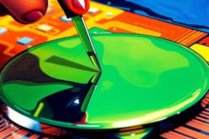
- Wafer Final Polishing: Achieves a mirror-like finish on one side, indicating contaminant-free status.
- Resistivity Check and Inspection: Ensures material quality before further processing.
Assignment
- Research paper should cover:
- History of Integrated Circuits.
- Various package types available.
- Example IC from any manufacturer and its applications.
- Advantages of using the selected IC.
Studying That Suits You
Use AI to generate personalized quizzes and flashcards to suit your learning preferences.