Podcast
Questions and Answers
What is the primary material used in the fabrication of MOS transistors?
What is the primary material used in the fabrication of MOS transistors?
- Gallium Arsenide
- Germanium
- Silicon (correct)
- Copper
What is the main purpose of the oxidation process in semiconductor manufacturing?
What is the main purpose of the oxidation process in semiconductor manufacturing?
- To minimize electron mobility
- To enhance the mechanical strength
- To create an insulating oxide layer (correct)
- To increase thermal conductivity
Which of the following steps is NOT part of wafer manufacturing?
Which of the following steps is NOT part of wafer manufacturing?
- Wafer Polishing
- Oxidation (correct)
- Wafer Cleaning
- Ingot Slicing
At what temperature range is the oxidation process typically carried out?
At what temperature range is the oxidation process typically carried out?
What role does SiO2 play in integrated circuits?
What role does SiO2 play in integrated circuits?
Why is silicon preferred over other materials for semiconductor fabrication?
Why is silicon preferred over other materials for semiconductor fabrication?
Which of the following processes is part of wafer manufacturing?
Which of the following processes is part of wafer manufacturing?
What does the process of oxidation help to isolate in semiconductor devices?
What does the process of oxidation help to isolate in semiconductor devices?
What is the primary characteristic of wet etching?
What is the primary characteristic of wet etching?
Which deposition technique is typically used for creating uniform layers on a semiconductor wafer?
Which deposition technique is typically used for creating uniform layers on a semiconductor wafer?
What distinguishes ion implantation from diffusion in the doping process?
What distinguishes ion implantation from diffusion in the doping process?
In which situation is diffusion generally used?
In which situation is diffusion generally used?
Which of the following layers can be deposited using Chemical Vapor Deposition (CVD)?
Which of the following layers can be deposited using Chemical Vapor Deposition (CVD)?
What is one key advantage of using ion implantation in semiconductor manufacturing?
What is one key advantage of using ion implantation in semiconductor manufacturing?
Which of the following statements is NOT true about dry etching?
Which of the following statements is NOT true about dry etching?
What role does temperature play in the diffusion doping process?
What role does temperature play in the diffusion doping process?
What is a significant advantage of ion implantation over diffusion in semiconductor manufacturing?
What is a significant advantage of ion implantation over diffusion in semiconductor manufacturing?
Which of the following processes involves introducing impurity ions at high velocity into a semiconductor material?
Which of the following processes involves introducing impurity ions at high velocity into a semiconductor material?
When is diffusion particularly preferred in semiconductor fabrication?
When is diffusion particularly preferred in semiconductor fabrication?
In the diffusion process, how does the dopant spread through the silicon wafer?
In the diffusion process, how does the dopant spread through the silicon wafer?
What impact does ion implantation typically have on semiconductor materials?
What impact does ion implantation typically have on semiconductor materials?
Which of the following is NOT a method used for doping via diffusion?
Which of the following is NOT a method used for doping via diffusion?
Which regions in a silicon wafer does diffusion primarily aim to create for MOSFET transistors?
Which regions in a silicon wafer does diffusion primarily aim to create for MOSFET transistors?
How do dopant atoms behave during the ion implantation process?
How do dopant atoms behave during the ion implantation process?
What is the main purpose of metal wiring in semiconductor manufacturing?
What is the main purpose of metal wiring in semiconductor manufacturing?
Which process is involved in the wafer dicing method?
Which process is involved in the wafer dicing method?
What is a primary function of IC packaging?
What is a primary function of IC packaging?
Which of the following processes is involved in metal wiring?
Which of the following processes is involved in metal wiring?
Why is the wafer dicing process critical in semiconductor manufacturing?
Why is the wafer dicing process critical in semiconductor manufacturing?
What aspect of IC packaging directly contributes to a semiconductor's longevity?
What aspect of IC packaging directly contributes to a semiconductor's longevity?
Which of the following best describes the role of annealing in the metal wiring process?
Which of the following best describes the role of annealing in the metal wiring process?
What type of machinery is essential for the wafer dicing process?
What type of machinery is essential for the wafer dicing process?
What is the purpose of oxidizing the wafer in the fabrication process?
What is the purpose of oxidizing the wafer in the fabrication process?
Which method allows dopant atoms to diffuse into the substrate?
Which method allows dopant atoms to diffuse into the substrate?
What role does photoresist play in the fabrication of n-wells?
What role does photoresist play in the fabrication of n-wells?
During the ion implantation process, how are the dopant ions introduced into the substrate?
During the ion implantation process, how are the dopant ions introduced into the substrate?
What is a consequence of lateral diffusion when forming n-wells?
What is a consequence of lateral diffusion when forming n-wells?
What type of material is used to form the transistor gates?
What type of material is used to form the transistor gates?
Why is the remaining oxide stripped away after the n-well formation?
Why is the remaining oxide stripped away after the n-well formation?
At what temperature range is the wafer typically oxidized?
At what temperature range is the wafer typically oxidized?
What is the primary function of layout design rules in manufacturing processes?
What is the primary function of layout design rules in manufacturing processes?
What does the symbol λ represent in scalable design rules?
What does the symbol λ represent in scalable design rules?
In a 180 nm process, what is the width of the polysilicon?
In a 180 nm process, what is the width of the polysilicon?
What is the minimum width and spacing for metal and diffusion in the conservative design rules for n-well processes?
What is the minimum width and spacing for metal and diffusion in the conservative design rules for n-well processes?
What must surround the contacts in design rules for n-well processes?
What must surround the contacts in design rules for n-well processes?
Which of the following services aggregates designs from various customers for low-cost prototyping?
Which of the following services aggregates designs from various customers for low-cost prototyping?
What is the relationship between feature size and λ in a manufacturing process?
What is the relationship between feature size and λ in a manufacturing process?
How does the use of scalable lambda-based design rules benefit designers?
How does the use of scalable lambda-based design rules benefit designers?
Flashcards
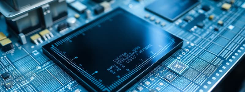
Semiconductor Manufacturing
Semiconductor Manufacturing
A crucial process for creating semiconductor devices like integrated circuits using CMOS technology on silicon wafers.
CMOS Technology
CMOS Technology
Complementary Metal-Oxide-Semiconductor, a fabrication method for transistors on silicon wafers.
Silicon Wafers
Silicon Wafers
Thin, flat disks of silicon used as substrates for building integrated circuits.
Wafer Manufacturing
Wafer Manufacturing
Signup and view all the flashcards
Oxidation (in Semiconductor)
Oxidation (in Semiconductor)
Signup and view all the flashcards
SiO2 (Silicon Dioxide)
SiO2 (Silicon Dioxide)
Signup and view all the flashcards
Integrated Circuits (ICs)
Integrated Circuits (ICs)
Signup and view all the flashcards
Ion Implantation
Ion Implantation
Signup and view all the flashcards
Metal Wiring
Metal Wiring
Signup and view all the flashcards
Wafer Dicing
Wafer Dicing
Signup and view all the flashcards
IC Packaging
IC Packaging
Signup and view all the flashcards
Wet Etching
Wet Etching
Signup and view all the flashcards
Dry Etching
Dry Etching
Signup and view all the flashcards
Deposition
Deposition
Signup and view all the flashcards
Chemical Vapor Deposition (CVD)
Chemical Vapor Deposition (CVD)
Signup and view all the flashcards
Physical Vapor Deposition (PVD)
Physical Vapor Deposition (PVD)
Signup and view all the flashcards
Ion Implantation
Ion Implantation
Signup and view all the flashcards
Diffusion
Diffusion
Signup and view all the flashcards
Ion Implantation
Ion Implantation
Signup and view all the flashcards
Diffusion
Diffusion
Signup and view all the flashcards
Dopant
Dopant
Signup and view all the flashcards
Semiconductor Doping
Semiconductor Doping
Signup and view all the flashcards
Ion Implantation Precision
Ion Implantation Precision
Signup and view all the flashcards
Diffusion Control
Diffusion Control
Signup and view all the flashcards
Dopant Profile
Dopant Profile
Signup and view all the flashcards
Impurity Ions
Impurity Ions
Signup and view all the flashcards
Inverter Cross-Section
Inverter Cross-Section
Signup and view all the flashcards
Fabrication Process
Fabrication Process
Signup and view all the flashcards
N-well
N-well
Signup and view all the flashcards
Oxidation
Oxidation
Signup and view all the flashcards
Photoresist
Photoresist
Signup and view all the flashcards
Etching
Etching
Signup and view all the flashcards
Dopants
Dopants
Signup and view all the flashcards
Diffusion (in Semiconductor)
Diffusion (in Semiconductor)
Signup and view all the flashcards
Ion Implantation
Ion Implantation
Signup and view all the flashcards
Polycrystalline silicon (Polysilicon)
Polycrystalline silicon (Polysilicon)
Signup and view all the flashcards
Layout Design Rules
Layout Design Rules
Signup and view all the flashcards
Lambda (λ)
Lambda (λ)
Signup and view all the flashcards
Feature Size
Feature Size
Signup and view all the flashcards
MOSIS
MOSIS
Signup and view all the flashcards
Minimum Width (Metal/Diffusion)
Minimum Width (Metal/Diffusion)
Signup and view all the flashcards
Minimum Spacing (Metal/Diffusion)
Minimum Spacing (Metal/Diffusion)
Signup and view all the flashcards
Contact Size
Contact Size
Signup and view all the flashcards
Polysilicon Width
Polysilicon Width
Signup and view all the flashcards
Polysilicon-Diffusion Overlap
Polysilicon-Diffusion Overlap
Signup and view all the flashcards
Polysilicon-Diffusion Spacing
Polysilicon-Diffusion Spacing
Signup and view all the flashcards
Study Notes
Semiconductor Manufacturing Process
- Semiconductor fabrication is crucial
- Fabrication is based on CMOS technology
- CMOS transistors are on silicon wafers
- Silicon is economical, better conductivity, less noise, and easier to format MOSFET transistors
- Silicon is the base material for MOS fabrication
Step-by-Step Fabrication Process
- Process transforms silicon wafers into functional chips
- Wafer manufacturing is a crucial stage in semiconductor industry
- Wafers are thin, flat disks that function as substrates for integrated circuits (ICs), sensors etc
- Key stages in wafer production:
- Raw material preparation (Si Ingot Production)
- Ingot Slicing
- Wafer Polishing
- Wafer Cleaning
Oxidation
- Oxidation creates an oxide layer (SiO2) or insulating layer to control current flow, isolate components, and boost device performance
- Oxidation furnace operates at 900-1200 degrees Celsius using H2O or O2
- SiO2 is used in bipolar and MOS transistors to isolate devices, provide surface passivation, and act as a barrier against impurity diffusion/implantation in substrates
- SiO2 acts as a component in MOS devices and a dielectric isolation layer between multilevel interconnect layers
Oxidation Techniques
- Thermal Oxidation - Basic process in IC fabrication. Used when low charge density level is required at the interface of silicon and oxide
- Wet Oxidation - Chemical vapor deposition for forming SiO2 layer on top of the metal layer in multilevel structures
- Plasma Oxidation
Lithography
- Lithography transfers geometric patterns from a mask onto a thin layer of radiation-sensitive material (resist) on a semiconductor wafer
- Photolithography uses e-beam and involves:
- Oxidation Layering
- Photoresist Coating
- Stepper Exposure
- Development and Bake
- Acid Etching
- Spin, Rinse, and Dry
Photomask Design
- Photomask is a master template for IC design
- Commonly 6-inch X 6-inch
- Uses quartz or glass substrates with opaque films for more complex masks
- Designs start as a file format, then created in photomask facilities
- Masks are used in lithography scanners to pattern desired features on wafers
Full Mask
- One layer = One mask
- Number of layers = Number of masks
Etching
- Etching removes unwanted materials from a wafer using chemicals or plasma after lithography
- Wet Etching: Selective removal of material using liquid etchants like acids, bases, or solvents
- Dry Etching: Material removal using plasma to selectively remove material on a substrate
Deposition
- Blanket of materials deposited on a surface using multiple techniques, such as:
- Selective Deposition
- Atomic-Layer Deposition
- Chemical Vapor Deposition (CVD)
- Physical Vapor Deposition (PVD)
- Type of technique depends on the semiconductor process node, type of chip, and time required for the deposition
- The deposition process must be uniform across the wafer
Doping
- Ion implantation and diffusion introduce dopants for semiconductor materials
- Ion Implantation: High-energy ion bombardment of dopants into semiconductor wafers for precise doping profiles in devices like CMOS
- Diffusion: Dopants diffused at high temperatures into semiconductor materials
Diffusion vs. Ion Implantation
- Ion Implantation: Precise control of dopant concentration and depth, but can damage the material and is more costly.
- Diffusion: Simpler, less expensive, but offers less control of dopant profile.
Diffusion
- Adds impurities (N-type or P-type) to silicon wafers for MOSFET transistor regions.
- Impurity (dopant) added to silicon using chemical sources at high temperatures
- Can also use doped oxide source, or ion-implanted source
Ion Implantation
- Process where impurity atoms are accelerated to high velocity and introduced into a single crystal substrate
- Impurity atoms enter lattice, colliding with existing atoms and gradually losing energy until rest at some depth
Metal Wiring
- Crucial process for creating electrical connections on wafers
- Involves depositing, patterning, and etching metal layers for functional electrical connections
- Techniques: metal deposition, lithography for patterning, etching, annealing to improve properties, testing to ensure quality
- The process is crucial for performance and reliability of semiconductor devices
Wafer Dicing
- Cuts a silicon wafer into individual components (chips/dies).
- Process is vital for integrated circuit and semiconductor devices fabrication
- Requires high-quality high precision machinery
IC Packaging
- Encapsulates the semiconductor device protecting it from corrosion and damage and allows mounting to printed circuit boards (PCB).
- Final stage in semiconductor production
- The package protects the IC from damage from external elements and corrosive effects of age
Common IC Package Types
- Pin-grid array (for socketing)
- Lead-frame and dual-in-line packages (for assemblies with pins through holes)
- Chip scale package (single-die, direct surface mountable with area less than 1.2X die area)
- Quad flat pack (leadless variety)
- Quad flat no-lead (tiny package, for surface mounting)
- Multichip package (incorporates multiple ICs, discrete components, and semiconductor dies on a substrate)
- Area array package (maximizes chip surface area for interconnections)
Testing
- Functional testing of fabricated semiconductor chips
- Crucial rules and considerations during the fabrication process:
- Design Rule Check (DRC)
- Scalable Design Rule
- Micron-Rules Process
- Circuit-Under-Test
- Packaging ICs Rules
- Cleanroom Environment
- Different fabrication methods used according to different types of semiconductor devices
Fabrication Process: Inverter
- Sequential steps in creating an inverter chip
- Crucial steps using photolithography to define layers of the chip, including n-well, polysilicon, n+ and p+ diffusion, contacts and metal.
Inverter Cross-Section
- Detailed internal structure of an inverter, showing transistors (nMOS and pMOS), substrate and well connections, layers, and materials.
Fabrication Process: Inverter Mask Set
- Hypothetical sequence of masks used to create an inverter, including n-well, polysilicon, and n+/p+ diffusion layers and metal layers
Fabrication Process: Cross-sections during n-well manufacturing process
- The method of adding dopants, diffusion and ion implantation.
- Diffusion and ion implantation methods for adding dopants
Fabrication Process: Cross-sections during polysilicon and n-diffusion manufacturing process
- Process of creating transistor gates.
- Using Chemical Vapor Deposition
- Patterned polysilicon masks for gates
Fabrication Process: Cross-sections during p-diffusion, contacts, and metal manufacturing process
- P-diffusion mask, oxide is used for masking, patterned, and contact cuts
- Sputtering aluminum for even metal coating
- Metal patterning techniques using metal masks
Layout Design Rules
- Rules for packing and arranging small features in manufacturing processes
- Scaling designs can be difficult across different processes or foundries
- Descriptors for processes: feature size, minimum drawn transistor channel length.
- Typical minimum transistors channel length is half of the feature size.
Layout Design Rules: Inverter
- The layout of transistors is important
- PMOS transistors are typically wider than N-MOS transistors because holes move slower than electrons.
Gate Layouts
- Line of diffusion, which consists of four horizontal strips: metal ground, n-diffusion, p-diffusion and metal power
- Power and ground called supply rails.
- Layout for inverter, showing well and substrate taps placed below power and ground rails.
- Line of diffusion rule widely used
Other
- Links to videos that can further explain the content and provide a better understanding of MOSFETs etc in more detail
Studying That Suits You
Use AI to generate personalized quizzes and flashcards to suit your learning preferences.


