Podcast
Questions and Answers
What is the primary function of linear integrated circuits in the field of telecommunications?
What is the primary function of linear integrated circuits in the field of telecommunications?
To achieve understanding and knowledge on the fundamental concepts of linear integrated circuits, their functions and applications.
The course aims to achieve understanding and knowledge on the fundamental concepts of linear integrated circuits.
The course aims to achieve understanding and knowledge on the fundamental concepts of linear integrated circuits.
True (A)
What is the first step in IC fabrication?
What is the first step in IC fabrication?
- Photolithography
- Silicon wafer preparation (correct)
- Epitaxial growth
- Oxidation
The starting form of silicon used by manufacturers of devices and integrated circuits is known as a what?
The starting form of silicon used by manufacturers of devices and integrated circuits is known as a what?
What is the typical range of diameters for silicon wafers used in integrated circuit manufacturing?
What is the typical range of diameters for silicon wafers used in integrated circuit manufacturing?
What are the three categories that IC's can be classified into?
What are the three categories that IC's can be classified into?
In the context of integrated circuits (ICs), what does 'SSI' stand for?
In the context of integrated circuits (ICs), what does 'SSI' stand for?
What are the two main types of integrated circuits?
What are the two main types of integrated circuits?
In what type of IC is the entire circuit built into a single piece of semiconductor chip?
In what type of IC is the entire circuit built into a single piece of semiconductor chip?
What is a key advantage of using silicon in semiconductor manufacturing?
What is a key advantage of using silicon in semiconductor manufacturing?
What is the primary purpose of the Czochralski process in IC fabrication?
What is the primary purpose of the Czochralski process in IC fabrication?
What is the purpose of lapping and polishing silicon wafers?
What is the purpose of lapping and polishing silicon wafers?
Epitaxial growth is a process used to deposit N on N+ silicon, which is impossible to accomplish by diffusion?
Epitaxial growth is a process used to deposit N on N+ silicon, which is impossible to accomplish by diffusion?
Name two functions of epitaxial processes between bipolar transistors?
Name two functions of epitaxial processes between bipolar transistors?
Which of the following is a key characteristic of SiO2 (silicon dioxide) as a passivating layer in silicon technology?
Which of the following is a key characteristic of SiO2 (silicon dioxide) as a passivating layer in silicon technology?
What acid is used to etch away exposed silicon dioxide during the photolithography process?
What acid is used to etch away exposed silicon dioxide during the photolithography process?
In wet etching, material is etched equally in all directions
In wet etching, material is etched equally in all directions
What is a common dopant for P-type layers in semiconductor manufacturing?
What is a common dopant for P-type layers in semiconductor manufacturing?
Which of the following is NOT an advantage of Ion Implantation?
Which of the following is NOT an advantage of Ion Implantation?
What material is commonly used for metallization in IC fabrication?
What material is commonly used for metallization in IC fabrication?
Flashcards
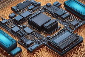
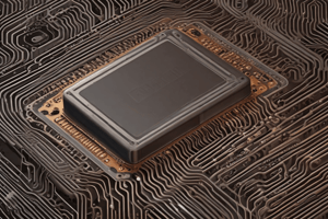
Integrated Circuits (ICs)
Integrated Circuits (ICs)
Miniaturized electronic circuits and systems on a single silicon wafer.
Discrete Units
Discrete Units
Discrete units are individual components like diodes and transistors.
Monolithic ICs
Monolithic ICs
Monolithic ICs have all components fabricated and interconnected on a single chip.
Hybrid ICs
Hybrid ICs
Signup and view all the flashcards
Advantage of Silicon (SiO2)
Advantage of Silicon (SiO2)
Signup and view all the flashcards
Wafer
Wafer
Signup and view all the flashcards
Silicon Requirements
Silicon Requirements
Signup and view all the flashcards
Scale of Integration
Scale of Integration
Signup and view all the flashcards
Types of ICs
Types of ICs
Signup and view all the flashcards
IC Disadvantages
IC Disadvantages
Signup and view all the flashcards
Czochralski Process
Czochralski Process
Signup and view all the flashcards
Seed Crystal
Seed Crystal
Signup and view all the flashcards
Lapping and Polishing
Lapping and Polishing
Signup and view all the flashcards
Epitaxial Growth
Epitaxial Growth
Signup and view all the flashcards
Passivating Layer SiO2 characteristics
Passivating Layer SiO2 characteristics
Signup and view all the flashcards
Thermal Oxidation of Silicon
Thermal Oxidation of Silicon
Signup and view all the flashcards
Wafer preparation in photolithography
Wafer preparation in photolithography
Signup and view all the flashcards
Etching
Etching
Signup and view all the flashcards
Wet etching
Wet etching
Signup and view all the flashcards
Dry etching
Dry etching
Signup and view all the flashcards
Pre-deposition Diffusion
Pre-deposition Diffusion
Signup and view all the flashcards
Drive-in Diffusion
Drive-in Diffusion
Signup and view all the flashcards
Ion Implantation Advantages
Ion Implantation Advantages
Signup and view all the flashcards
Isolation Techniques
Isolation Techniques
Signup and view all the flashcards
Metallization
Metallization
Signup and view all the flashcards
Why Aluminum is preferred for metallization:
Why Aluminum is preferred for metallization:
Signup and view all the flashcards
Testing for Reliability
Testing for Reliability
Signup and view all the flashcards
Assembly processing & packaging
Assembly processing & packaging
Signup and view all the flashcards
Scribing and Cleaving
Scribing and Cleaving
Signup and view all the flashcards
IC package configurations
IC package configurations
Signup and view all the flashcards
Study Notes
- The learning outcome is to illustrate the manufacturing process of Integrated Circuits (ICs).
- The course aims to provide understanding of linear integrated circuits.
- Students will explore simulation software to reinforce theoretical and practical skills.
- The manufacturing process of ICs is discussed.
Course Objectives
- Explain ideal and practical Op-Amp characteristics, including compensation parameters.
- Design and analyze linear and nonlinear circuits using Op-Amps.
- Analyze and design Phase-Locked Loop (PLL), Analog-to-Digital Converter (ADC), and Digital-to-Analog Converter (DAC) circuits.
- Design and simulate real-time application circuits with special function ICs.
Course Learning Outcomes
- Ability to explain the manufacturing process of Integrated Circuits (ICs).
- Applying knowledge of differential amplifiers with op amp characteristics.
- Design linear and non-linear applications of operational amplifiers.
- Construct analog circuits using PLL for AM and FM detection, FSK modulation and demodulation, including Frequency synthesizing and clock synchronization.
- Analyze and design both A/D and D/A converters.
- Design application-oriented circuits using special function ICs for voltage regulation, tuned amplifiers, and optocouplers.
- Comprehension of electronics production influences on global heating and resource consumption and application of life-cycle analysis.
Assessment Plan
- Quiz: 10%
- Attendance and HSE: 5%
- Aim/Objectives, Procedure, Table, Graphs, & Results: 10%
- Lab Test: 10%
- Case Study: 10%
- Midterm Exam (1 Hour): 20%
- Final Exam (2 Hours): 35%
Outline of Topics
- Introduction to Integrated Circuits.
- Reason for using Silicon in IC manufacturing.
- Purity standards for Silicon.
- Classification of ICs.
- Scale of Integration.
- Types of Integrated Circuits.
- Advantages and Disadvantages of ICs.
- Steps Involved in IC Fabrication.
Introduction to Semiconductor Devices and Integrated Circuits
- Silicon is a common semiconductor material used as a substrate.
- Silicon wafers are an inexpensive material option for solar cells.
- Compound semiconductors like IV-IV, III-V, and II-VI are now a main focus area.
- Compound semiconductor III-V is broadly used in LEDs and lasers with gallium arsenide (GaAs), indium phosphide (InP), gallium phosphide (GaP), gallium nitride (GaN) and aluminum nitride (AlN).
- Most optoelectronic devices use the III-V compound.
- Microminiaturization of electronics allowed innovations in computers and communications in the 20th century.
- New applications became viable that were impossible before with discrete devices.
- Integrated circuits on silicon wafers followed by increased wafer size reduced costs and improved reliability.
Why Silicon?
- Semiconductor devices either come in the form of: Discrete Units or Integrated Units.
- Discrete Units include diodes and transistors.
- Integrated Circuits use discrete units to make a singular device.
- Integrated Circuits come in 2 forms: Monolithic and Hybrid.
- Monolithic ICs fabricate and interconnect transistors, diodes, and resistors on the same chip.
- Hybrid ICs have discrete external elements connected to the chip.
- Germanium and gallium arsenide have special problems/challenges, while silicon has advantages.
- Silicon is abundant as sand, which is a major advantage.
- Silicon dioxide (SiO2) can be formed, which means it has excellent insulating properties.
- Gallium arsenide crystals have numerous crystal defects, limiting device effectiveness.
- GaAs is more difficult to grow in crystal form.
- Silicon and germanium do not decompose during processing like gallium arsenide can.
- Silicon is the major semiconductor in the industry at this current point in time.
The Purity of Silicon
- The starting form of silicon is a circular slice known as a wafer.
- Wafer diameters range from 10-20 cm, and can reach up to 30 cm.
- Silicon is abundant in nature within sand and quartz.
- Silicon must be crystalline, pure, free of defects, and uncontaminated.
Classification of Integrated Circuits
- Integrated circuits are classified based on Scale of Integration, Types of Signal, and Types of Fabrication Techniques.
- Classifications by Scale of Integration consists of SSI, MSI, LSI, VLSI and ULSI.
- SSI has less than 10 components.
- MSI has 10-100 components.
- LSI has 100-1000 components.
- VLSI has 1000-10,000 components.
- ULSI has over 100,000 components.
- Signal Types consists od Digital ICs and Analog/Linear ICs.
- Type of Fabrication Technique: Monolithic ICs, Thick-Thin ICs and Hybrid ICs.
Scale of Intergration
- The first semiconductor IC chip had just one diode/transistor.
- Small-scale integration (SSI) was the first arrival.
- Improvements led to large-scale integration (LSI)
Types of Integrated Circuits
- Two types of ICs are monolithic and hybrid.
- Monolithic ICs build the entire circuit on a single semiconductor chip with active and passive components.
- Microprocessors and memory ICs are the most common integrated circuits and examples of monolithic ICs.
- Hybrid ICs integrate the electronic circuit in a ceramic substrate with several components in a single package.
- Hybrid ICs consist of multiple monolithic ICs connected by metallic interconnects on a common substrate.
- Hybrid IC technology bonds substrates at either the die or wafer level using methods which streamlines connections and uses less wire bonding.
- Hybrid ICs streamline process, decreases costs, increases communications and produces higher system yield.
Advantages and Disadvantages of ICs
- The dimensions of ICs is small, which means the overall size is low.
- Integrated circuits are of low weight due to very small size.
- Low power is needed due to the lower dimensions.
- Large-scale production, which means low cost to manufacture.
- High reliability if there is an absence of solder joints.
- Facilitates integration of large number of devices.
- Improves the device performance at high-frequency regions.
- IC resistors have a limit range.
- Inductors cannot be formed using IC.
- Transformers cannot be formed using IC.
Steps Involved in IC Fabrication
- Silicon wafer or substrate preparation.
- Epitaxial growth.
- Oxidation.
- Photolithography.
- Diffusion.
- Ion implantation.
- Isolation technique.
- Metallization.
- Assembly processing and packaging.
Crystal Growth and Wafer Preparation
- The Czochralski Process grows crystals by starting with pure semiconductor grade silicon melted in a lined graphite crucible.
- The melt is held at a temperature of 1690K, which is greater than the melting point (1685K) of silicon.
- After developing the melt, a small, highly perfect crystal is attached to a holder possessing a desired crystal orientation, and then dipped into the melt to allow slight part to melt.
- Crystal growth and wafer preparation is crucial in device fabrication.
- The Czochralski process is commonly used in crystal growth.
- A small silicon seed crystal is attached to a rod and is lowered into a crucible of molten silicon where acceptor impurities were added.
- Controlled pulling grows a single p-type or n-type crystal ingot.
- The ingot is sliced into round wafers for component fabrication.
- One wafer side is lapped and polished to eliminate surface imperfections.
- State-of-the-art crystals are 200 mm for modern chip manufacture.
- Crystal diameter is decreased until a point contact is made with the melt, which then cools and is removed.
- Ingots can be 200-300mm, reaching lengths od 100cm.
- High-precision equipment is required.
- Smooth and totally flat slices must be produced with zero damage to the crystal structure.
- The wafers need to be subjected to lapping, polishing, and chemical etching.
- The wafers get cleaned, rinsed and dried for use in discrete devices and integrated circuits fabrication.
Epitaxial Growth
- Epitaxial growth technology uses the hydrogen reduction of gases like silane (SiH4) or silicon tetrachloride (SiCl4) as the silicon source.
- Silane requires a lower operating temperature and delivers a faster growth rate than silicon tetrachloride.
- Chemical reaction for SiCl4 hydrogen reduction is: SiCl4 + 2H2 → Si + 4HCl at 1200 °C
- Chemical reaction for SiH4 hydrogen reduction is: SiH4 → Si +2H2 within H2 atmosphere at 1000°C
- An n-type epitaxial layer, around nanometre to micrometre thick, becomes a p-type substrate that measures resistivity of a few cm approximately.
- Epitaxial films are required, so impurities must be added like Phosphine (PH3) and Diborane (B2H6) to be added to the underlying silicon substrate.
Epitaxy Operations
- Epitaxy deposits N on N+ silicon, which is not possible by diffusion.
- Epitaxy provides isolation between bipolar transistors by depositing N- on Phosphorus(P).
- Heat wafer to 1200°C.
- H2 reduces SiO2.
- Vapor-etch the surface with anhydrous HCl to remove silicon and contaminants.
- Turn off HCl.
- Drop the temperature to 1100°C.
- Turn on silicon tetrachloride (SiCl4).
- Introduce dopant.
Oxidation
- Silicon can grow an oxide layer on the SiO2 layer.
- SiO2 performs as a passivation layer, and does not allow the silicon to penetrate n-type Si wafer.
- Masking leads to precise doping inside particular regions of a chip.
- Hydrogen fluoride (HF) is capable of being etched.
- Thermal oxidation of silicon, also called wet oxidation, occurs with water vapor present The chemical reaction is: Si + 2H2O → SiO2 + 2H2
- Thickness is in range of 0.02 mm to 2 mm
- Temperature, impurity concentration and processing time influence thickness.
- Dry oxidation occurs with oxygen as a thin layer of oxide which is called the thermal oxide (silicon dioxide) and is commonly made in excess of 1000°C silicon substrate temperatures.
- Silicon dioxide films are used to shield by stopping diffusion of atoms, or to drive them in specific spots.
Photolithography Baking
- The wafer is baked at 100°C to solidify the resist which in turn is baked into the wafer.
- The reticle is placed on the wafer, and it is auto aligned through computer control.
- The reticle is exposed to UV light, which passes through the reticle, and light from the underlying opaque regions don't affect it.
- Exposed photoresist is chemically removed by using an organic solvent and exposing the underneath silicon dioxide.
- The process is similar to what is used when photographic film is being developed.
- Hydrofluoric acid which dissolves silicon dioxide (does not dissolve silicon) etches exposed silicon dioxide.
- Silicon dioxide and photoresist still covers opaque reticle parts.
- Stripping is done with the proper solvents.
Etching Tecgniques
- The selective semiconductor, metal, and silicon dioxide removal is etching.
- Etching has 2 types: wet and dry.
- Wet etching involves chemical immersion into a chemical solution at a predetermined temperature.
- The unwanted material is removed equally, which is problematic when dealing with small objects.
- Dry etching involves the submersion of wafers into gaseous plasma.
- Plasma is generated through a electrode with a radio-frequency electric field.
- Electrodes gain kinetic energy so that plasma can occur, atoms on surface get removed when transferred from the ions to the atoms.
Diffusion
- Processes occur in two steps: predeposition and drive-in diffusion.
- Predeposition: introduced with dopant atoms surface at 1000°C temperature.
- In recent years, ion implantation is used here instead.
- Temperature above 1000°C causes silicon atoms to move from high density, which breaks the bond with neighboring atoms.
- Drive in process means deeper surfaces.
- Boron for P-type layers and phosphorus, antimony, and arsenic are common dopants for N-type layers.
- Wafers are put into quartz furnace tube with surrounding surrounding resistance heaters.
- The wafers are put into a slotted carrier (boat).
- To introduce a phosphorus dopant, use phosphorus oxychloride.
Ion Implantation
- Ions are generated through arc discharge within phosphine (PH3), which contain: phosphorus.
- The ions are accelerated in an electric field to reach 20keV, then it goes through a strong magnetic field.
- Unwanted impurities are generated with arc discharge so the magnetic field operates to separate impurities from the dopant ions and depending on the mass of the deflection.
- Following this separation, the ions get accelerated to hundreds of keV so they can target the surface.
Advantages of Ion Implantation
- Doping levels can be precisely controlled.
- The depth of the dopant can be easily regulated.
- Extreme dopant is guarantee.
- The doping across the surface is accurately controlled.
- There is little spread of the beam and the doping area is defined because ions are sent in a directed beam.
- Impurities get minimized because it is considered a low temperature process.
Isolation Techniques
- Its in necessary to provide electrical isolation between different components and connections.
- Common techniques are p-n junction and dielectric isolation.
- P-N JUNCTION ISOLATION means impurities diffuse.
- Dielectric isolation has components surrounded by SiO2 which means the components and connections are protected between electrical isolation.
- Isolating reduces capacitance through dielectric layer thickness, and enables the the fabrication of PNP and NPN transistors.
Metallization
- The thin metal film layer is metallization so that the various components and connections can can connect.
- At the end of the fabrication process, metallization takes place and deposition becomes easier.
- Aluminum is good for conducting current.
- Aluminum makes mechanical bonds with silicon.
- Contacting the wafer with aluminum means it is a low electricity resistance environment.
- Etching and deposition can both be single processes.
Considerations for Reliability Testing
- Testing thoroughly to show that it fabricated through all the processes successfully.
- IC's fabricated though batch processing may not perform up to par so it is key to perform a secondary testing.
- Electronic testers press probes into IC surface to test functionally.
Assembly Processing and Packaging
- Scribing and cleaving are processes to separate chips (wafers contain multiple units)
- Diamond tipped tool can create cuts with rectangular grid in order to separate units.
- There are 3 configuration packages which are: metal can package, ceramic flat package, and dual in line package.
- Last step involves packaging per dimensional requirement.
- After approval, dies break into little individual pieces.
- small wires connect to connection pins.
- Dual input is a common packaging solution used with most digital ICs.
Planar Resistance Fabrication
- An N+ substrate grown through the Czochralski method to start.
- The layer is a 1-5 micron thick deposit created thorough epitaxy.
- Surface becomes coated.
- An oxidized silicon dioxide layer is used.
- After coating with photoresist, a mask gets placed along silicon surface and exposure starts.
- Remove the mask, remove the resist, and etch the silicon .
- Once Boron is diffused a P-type zone forms.
- Deposited is a thin layer of aluminum film, and metalized areas are given resist and areas for metal can be covered.
- Surface gets etched in removal the resist of leftover metallic compounds.
- At the back surface, metal is deposited as result of heat.
Points to Remember
- Monolithic circuits build everything on a single semiconductor chip of active components with circuit performance based off the semiconductor properties.
- Hybrid integrated circuits apply the usage of semiconducting technology to allow the connection of all individual ICs together.
- Hybrid integrated circuits create possibilities for brand electrical, heat and mechanical bonding.
- Integration circuits boost bandwidth, create modular chips and have great system yields.
- Integrated circuits offer improved yields with more bandwidth.
- The Czochralski method creates ingots.
- With an exact material, the epitaxial form creates single crystal silicon.
- For diffusion is substrate layers steps.
- The wafer is targeted at high speeds of voltage.
- Metallization causes intersections of the components and elements to take place.
- Circuit testing has happen prior to packaging.
Studying That Suits You
Use AI to generate personalized quizzes and flashcards to suit your learning preferences.
Related Documents
Description
Learn about the manufacturing process of Integrated Circuits (ICs). Explore ideal and practical Op-Amp characteristics, including compensation parameters. Design and analyze linear and nonlinear circuits, as well as Phase-Locked Loop (PLL), Analog-to-Digital Converter (ADC), and Digital-to-Analog Converter (DAC) circuits.