Podcast
Questions and Answers
What is the traditional method for PCB assembly?
What is the traditional method for PCB assembly?
- Surface Mount Technology (SMT)
- Dual In-Line (DIL) leadframe mounting
- Direct Chip Attach (DCA)
- Through Hole / Pin Through Hole (TH/PTH) Technology (correct)
What is the pitch of the pins on a standard Dual In-Line (DIL) integrated circuit?
What is the pitch of the pins on a standard Dual In-Line (DIL) integrated circuit?
- 0.05 inches
- 0.2 inches
- 0.1 inches (correct)
- 0.5 inches
Which DIL package would typically have the widest width?
Which DIL package would typically have the widest width?
- DIL 14
- DIL 40
- DIL 64 (correct)
- DIL 24
What are the advantages of using Surface Mount Technology (SMT) compared to Through Hole Technology?
What are the advantages of using Surface Mount Technology (SMT) compared to Through Hole Technology?
What is the typical width of a DIL 20 pin package?
What is the typical width of a DIL 20 pin package?
What is the typical pitch of a Quad Flat Pack (QFP) 208 SMT IC package?
What is the typical pitch of a Quad Flat Pack (QFP) 208 SMT IC package?
According to Rent's rule, what happens to the number of leads (Nleads) if the number of transistors (Ntransistors) in a microprocessor increases by a factor of 10?
According to Rent's rule, what happens to the number of leads (Nleads) if the number of transistors (Ntransistors) in a microprocessor increases by a factor of 10?
Which of the following is considered a passive electronic component?
Which of the following is considered a passive electronic component?
What is the typical pitch for through-hole ICs?
What is the typical pitch for through-hole ICs?
What is a common method for delivering SMT 'chip' components?
What is a common method for delivering SMT 'chip' components?
What does the '12' in a '1206' chip component size designator indicate?
What does the '12' in a '1206' chip component size designator indicate?
What are local fiducials primarily used for in SMT assembly?
What are local fiducials primarily used for in SMT assembly?
Which type of through-hole component is commonly supplied in a bandolier?
Which type of through-hole component is commonly supplied in a bandolier?
What is the primary factor driving the shift from Through Hole (TH) to Surface Mount Technology (SMT)?
What is the primary factor driving the shift from Through Hole (TH) to Surface Mount Technology (SMT)?
What is a common pitch dimension for pins on a Dual In-Line (DIL) integrated circuit?
What is a common pitch dimension for pins on a Dual In-Line (DIL) integrated circuit?
A DIL integrated circuit with a width of 0.6 inches is most likely to have how many pins?
A DIL integrated circuit with a width of 0.6 inches is most likely to have how many pins?
What is a key dimensional characteristic that distinguishes different DIL packages?
What is a key dimensional characteristic that distinguishes different DIL packages?
What is the width of a DIL 64 package?
What is the width of a DIL 64 package?
Which of the following best describes a key attribute of Through Hole (TH) components, in contrast to SMT?
Which of the following best describes a key attribute of Through Hole (TH) components, in contrast to SMT?
Compared to Dual In-Line (DIL) packages, what is a significant advantage of Surface Mount Technology (SMT) components?
Compared to Dual In-Line (DIL) packages, what is a significant advantage of Surface Mount Technology (SMT) components?
What distinguishes a DIL 14 package from other DIL packages?
What distinguishes a DIL 14 package from other DIL packages?
What impact did the invention and development of SMT have on the manufacturing of electronic devices?
What impact did the invention and development of SMT have on the manufacturing of electronic devices?
What is a Dual In-Line (DIL) package primarily designed for?
What is a Dual In-Line (DIL) package primarily designed for?
Which of the following describes an area array package?
Which of the following describes an area array package?
What is the relationship between the number of transistors and the number of leads in a microprocessor, according to Rent's rule?
What is the relationship between the number of transistors and the number of leads in a microprocessor, according to Rent's rule?
Which of the following is NOT a typical physical form for components?
Which of the following is NOT a typical physical form for components?
In the context of component packaging for automated assembly, what is a 'bandolier'?
In the context of component packaging for automated assembly, what is a 'bandolier'?
What is a key distinguishing characteristic of Metal Electrode Leadless Face (MELF) components?
What is a key distinguishing characteristic of Metal Electrode Leadless Face (MELF) components?
What is the primary purpose of local fiducials on a PCB?
What is the primary purpose of local fiducials on a PCB?
What is the approximate pitch of a BGA 304 package?
What is the approximate pitch of a BGA 304 package?
What is the significance of the '06' in a '1206' chip component size?
What is the significance of the '06' in a '1206' chip component size?
What is the function of the gantry system in an SMT pick-and-place machine?
What is the function of the gantry system in an SMT pick-and-place machine?
What is a common packaging method for delivering Surface Mount Technology (SMT) components?
What is a common packaging method for delivering Surface Mount Technology (SMT) components?
Which of the following best describes the primary function of the substrate material in a PCB?
Which of the following best describes the primary function of the substrate material in a PCB?
What is a key characteristic of a substrate material with good dielectric properties for use in high-frequency circuits?
What is a key characteristic of a substrate material with good dielectric properties for use in high-frequency circuits?
What is the typical material used for the substrate of a standard PCB?
What is the typical material used for the substrate of a standard PCB?
In the context of PCB manufacturing, what does 'electroless copper' refer to?
In the context of PCB manufacturing, what does 'electroless copper' refer to?
What is the role of plated copper in the manufacturing of a double-sided plated through-hole (PTH) PCB?
What is the role of plated copper in the manufacturing of a double-sided plated through-hole (PTH) PCB?
What is the purpose of applying photoresist during PCB manufacturing?
What is the purpose of applying photoresist during PCB manufacturing?
What is the immediate next step after applying photoresist to a PCB in the manufacturing process?
What is the immediate next step after applying photoresist to a PCB in the manufacturing process?
What is the significance of the plating step in the manufacturing of a double-sided PTH PCB?
What is the significance of the plating step in the manufacturing of a double-sided PTH PCB?
Which of these steps is typically performed last in the manufacturing of a double-sided PTH PCB?
Which of these steps is typically performed last in the manufacturing of a double-sided PTH PCB?
Which process is used to remove unwanted copper from a PCB after imaging and resist development?
Which process is used to remove unwanted copper from a PCB after imaging and resist development?
What is the typical thickness of a copper layer in PCB manufacturing, expressed as weight per square foot?
What is the typical thickness of a copper layer in PCB manufacturing, expressed as weight per square foot?
Which of the following materials is commonly used for flexible PCBs?
Which of the following materials is commonly used for flexible PCBs?
What is the primary purpose of the holes drilled in a printed circuit board?
What is the primary purpose of the holes drilled in a printed circuit board?
What material are PCB drill bits typically made of?
What material are PCB drill bits typically made of?
What is a typical range of spindle speeds used in PCB drilling for small holes?
What is a typical range of spindle speeds used in PCB drilling for small holes?
Which method of hole formation is described as being high volume, low quality, and low complexity?
Which method of hole formation is described as being high volume, low quality, and low complexity?
During PCB lithography, what is the role of a photoresist?
During PCB lithography, what is the role of a photoresist?
In lithography, what does the exposure time depend on, given that $W = J/s$?
In lithography, what does the exposure time depend on, given that $W = J/s$?
What type of etching is best suited to produce fine, high-precision features in certain materials?
What type of etching is best suited to produce fine, high-precision features in certain materials?
What does '1oz' typically refer to in the context of PCB manufacturing?
What does '1oz' typically refer to in the context of PCB manufacturing?
Flashcards
Through Hole (TH) Technology
Through Hole (TH) Technology
The traditional PCB assembly process, where components with leads are inserted into holes drilled through the PCB and soldered on the other side.
Dual In Line (DIL)
Dual In Line (DIL)
A type of through-hole IC package where pins are arranged on opposite sides of the device in two parallel rows.
Pin Pitch
Pin Pitch
The spacing between the pins on a DIL package.
DIL Width
DIL Width
Signup and view all the flashcards
Surface Mount Technology (SMT)
Surface Mount Technology (SMT)
Signup and view all the flashcards
Quad Flat Pack (QFP)
Quad Flat Pack (QFP)
Signup and view all the flashcards
Ball Grid Array (BGA)
Ball Grid Array (BGA)
Signup and view all the flashcards
Rent's Rule
Rent's Rule
Signup and view all the flashcards
Passive Components
Passive Components
Signup and view all the flashcards
Active Components
Active Components
Signup and view all the flashcards
Pick and Place
Pick and Place
Signup and view all the flashcards
Dual In Line (DIL) Package
Dual In Line (DIL) Package
Signup and view all the flashcards
IC Packaging
IC Packaging
Signup and view all the flashcards
Quad Flat Pack (QFP) Package
Quad Flat Pack (QFP) Package
Signup and view all the flashcards
Ball Grid Array (BGA) Package
Ball Grid Array (BGA) Package
Signup and view all the flashcards
Pick and Place Machine
Pick and Place Machine
Signup and view all the flashcards
Axial Through Hole
Axial Through Hole
Signup and view all the flashcards
Radial Through Hole
Radial Through Hole
Signup and view all the flashcards
Chip Components
Chip Components
Signup and view all the flashcards
PCB Substrate
PCB Substrate
Signup and view all the flashcards
FR4
FR4
Signup and view all the flashcards
Dielectric Strength
Dielectric Strength
Signup and view all the flashcards
Dielectric Constant
Dielectric Constant
Signup and view all the flashcards
Dielectric Loss
Dielectric Loss
Signup and view all the flashcards
PCB Drilling
PCB Drilling
Signup and view all the flashcards
Photolithography
Photolithography
Signup and view all the flashcards
UV Lithography
UV Lithography
Signup and view all the flashcards
Etching
Etching
Signup and view all the flashcards
Plating
Plating
Signup and view all the flashcards
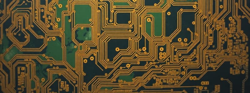
PCB Conductor
PCB Conductor
Signup and view all the flashcards
Copper Weight (oz/ft²)
Copper Weight (oz/ft²)
Signup and view all the flashcards
Multi-Spindle PCB Drilling
Multi-Spindle PCB Drilling
Signup and view all the flashcards
PCB Lithography
PCB Lithography
Signup and view all the flashcards
Photoresist Contrast
Photoresist Contrast
Signup and view all the flashcards
PCB Etching
PCB Etching
Signup and view all the flashcards
PCB Plating
PCB Plating
Signup and view all the flashcards
PCB Alignment
PCB Alignment
Signup and view all the flashcards
Study Notes
Electronics Manufacturing
- This topic covers manufacturing technologies of electronic components and printed circuit boards (PCBs).
- The lecturer is Patrick Webb, [email protected], T2.28b.
- Course code: 21WS610META.
Topics Outline
- Introduction: Discusses current technology trends and the specifics of electronics manufacturing.
- Interconnection requirements/hierarchies: Explores the necessary connections and their organization within electronic systems.
- Component types and their manufacture: Examines different components and their production methods.
- PCB manufacturing processes: Details processes like photolithography, drilling, and etching for PCB production.
- PCB assembly: Explains techniques like soldering to assemble PCBs.
- Contamination control/yield/testing: Discusses maintaining quality through control of contamination and yield measures, along with verification/validation.
Topic 3: Component Packaging and PCB assembly methods
- This section covers the procedures for packaging components and assembling PCBs.
- Images display various assembly technologies (diagrams of component placements and structures).
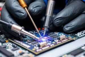
Through Hole/Pin Through Hole (TH/PTH) Technology
- This is a traditional PCB assembly method.
- It involves inserting components through holes in the PCB.
- Components are soldered to the PCB's conductor to complete the connection.
Dual In Line (DIL) TH ICs
- DIL refers to a dual in-line package.
- Various DIL package sizes (e.g., DIL 14, DIL 20, DIL 24, DIL 40, DIL 64) are discussed, including their respective pitches and widths.
- The 0.1" pitch is a standardized measurement (2.54mm).
- Examples show the image and dimensions of those types.
Dual In Line (DIL) Leadframe
- DIL package structures using leadframes or similar methods are considered.
SMT IC packages
- Surface Mount Technology (SMT) involves mounting components directly on the surface of PCBs instead of through holes.
- The following package types are discussed, including:
- JLCC 68: 0.05" pitch (~1.3mm).
- QFP 208 (Quad Flat Pack): 0.5 mm pitch.
- QFP 256: 0.4 mm pitch.
- BGA 225 (Ball Grid Array): 1.5 mm pitch.
- BGA 304: 1.25 mm pitch.
Rent's Rule Revisited
- Rent's rule is a guideline relating the number of pins (leads) to the number of transistors in a microprocessor.
- Increasing the transistor count by a factor of 10 generally doubles the number of leads, as indicated by the formula: Nleads = 2.4 x Ntransistors0.3.
Components and PCB assembly
- Electronic components are broadly categorized into passive and active types.
- Passive: Resistors (Rs), Capacitors (Cs), Inductors (Ls).
- Active: Diodes (Ds), Transistors (Ts or Qs), Integrated Circuits (ICs).
Physical form
- Component physical form varies depending on assembly type (through-hole or surface-mount).
System size and weight
- System size and weight are mainly determined by packaging and interconnection.
- For example, a typical PC motherboard is roughly 30 cm x 25 cm (750 cm2).
- Silicon (Si) content is typically around 10 cm2.
SMT Pick and Place Machine
- These machines automate the placement of SMT components on PCBs.
- Component placement speeds often exceed 12,000 components per hour.
Component Presentation
- Components are frequently presented in tape and reel packaging.
Axial through hole components
- Often used for resistors (Rs) and diodes (Ds).
- Components generally have two wires on a common axis arranged in a bandolier.
Radial through hole components
- Usually used for capacitors (Cs), transistors (Ts), and LEDs.
- Often supplied in a taped format with sprocket holes for proper handling.
Through hole ICs
- These integrated circuits (ICs) typically have four or more connection points arranged in two rows.
- Pitch is usually 0.1” (2.54mm)
- ICs of this type are usually packaged in sticks or tubes.
SMT Components
- “Chip” components (like resistors (Rs) and capacitors (Cs)) are abundant in SMT configurations.
- Typically packaged in bulk or on tape reels.
Evolution of chip component size
- Charts illustrate trends in chip component size over time. Various package sizes (0805, 1206, 0603) and dimensions (millimeters) are presented.
Other SMT components
- Metal electrode leadless face (MELF) packages (often containing resistors (Rs) and diodes (Ds)).
- Diverse IC package styles (e.g., SO, J-lead, QFP).
- Components can be supplied in tubes, tape, or trays.
Local fiducials
- Used with vision systems to accurately position components for fine pitch components on PCBs.
Studying That Suits You
Use AI to generate personalized quizzes and flashcards to suit your learning preferences.