Podcast
Questions and Answers
What does the term 'PTH' stand for in PCB vocabulary?
What does the term 'PTH' stand for in PCB vocabulary?
- Plated Through Hole (correct)
- Pathway to Hardware
- Printed Tool Holder
- Plate Thickness Height
Which feature of a hole is indicated by the term 'Annular Ring' in PCB vocabulary?
Which feature of a hole is indicated by the term 'Annular Ring' in PCB vocabulary?
- Hole depth measurement
- Hole location on the PCB
- Hole diameter tolerance
- Conductive material surrounding the hole (correct)
What is the purpose of a 'Coupon' in PCB manufacturing?
What is the purpose of a 'Coupon' in PCB manufacturing?
- Determine PTH copper thickness (correct)
- Indicate manufacturing date
- Check PCB color accuracy
- Measure hole diameter
What does a 'Date Code' on a PCB indicate?
What does a 'Date Code' on a PCB indicate?
In PCB terminology, what does 'NPTH' refer to?
In PCB terminology, what does 'NPTH' refer to?
What does the IPC standard tolerance for PTH size specify?
What does the IPC standard tolerance for PTH size specify?
What quality aspect does a 'Coupon' help determine in PCB manufacturing?
What quality aspect does a 'Coupon' help determine in PCB manufacturing?
'PTH' and 'NPTH' are terms commonly associated with which feature on a PCB?
'PTH' and 'NPTH' are terms commonly associated with which feature on a PCB?
'Annular Ring' in PCB vocabulary surrounds which part of a hole?
'Annular Ring' in PCB vocabulary surrounds which part of a hole?
What is the purpose of peelable solder mask in PCB manufacturing?
What is the purpose of peelable solder mask in PCB manufacturing?
Which finish is an alternative to HASL finish in PCB manufacturing?
Which finish is an alternative to HASL finish in PCB manufacturing?
What is the function of carbon pads/contacts on a PCB?
What is the function of carbon pads/contacts on a PCB?
How is the HASL finish applied to exposed copper features on bare circuit boards?
How is the HASL finish applied to exposed copper features on bare circuit boards?
In what scenario would you typically use peelable solder mask in PCB manufacturing?
In what scenario would you typically use peelable solder mask in PCB manufacturing?
What distinguishes OSP finish from HASL finish in PCB manufacturing?
What distinguishes OSP finish from HASL finish in PCB manufacturing?
What does the application of carbon pads/contacts aim to achieve in a PCB?
What does the application of carbon pads/contacts aim to achieve in a PCB?
Which process involves leveling the HASL finish with high-velocity hot air?
Which process involves leveling the HASL finish with high-velocity hot air?
What distinguishes peelable solder mask from regular solder mask in PCB manufacturing?
What distinguishes peelable solder mask from regular solder mask in PCB manufacturing?
Which feature of OSP finish makes it an attractive alternative to HASL finish in PCB manufacturing?
Which feature of OSP finish makes it an attractive alternative to HASL finish in PCB manufacturing?
Flashcards are hidden until you start studying
Study Notes
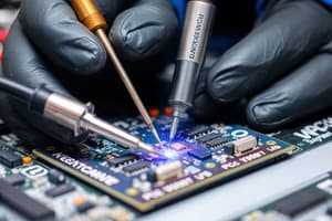
PCB Manufacturing Process
- The core material consists of a fiberglass and epoxy matrix, laminated on both sides with a thin sheet of copper.
- The circuit pattern is defined using a light-sensitive photo polymer, also known as photo resist, laminated on both sides of the core material.
- The photo tools with a negative image of the circuit pattern are created from the CAD data, aligned to the panel, and exposed to a measured amount of light, which polymerizes the exposed portions of the photo resist.
- The developing process removes the un-polymerized photo resist, leaving the circuit pattern defined by the polymerized photoresist.
Copper Pattern Formation
- Electro plating deposits about 0.001" of copper to all exposed metal areas of the panel, including surface features and hole wall interiors.
- Tin plating deposits a thin layer of Tin to all exposed copper areas, serving as an etch resist during the copper etch process.
Copper Etching
- The base copper is chemically etched away, with the circuit pattern and holes protected by the Tin plate during the etch process.
- The Tin plate is then chemically removed, exposing the base copper.
Solder Mask Application
- Solder mask is selectively applied to the panel, with proper clearance given to all appropriate surface features.
- The solder mask is then cured thermally.
Surface Finish
- The surface finish can be HASL (Hot Air Solder Level), Silver, OSP (Organic Solderability Preservative), or ENIG (Electroless Nickel Immersion Gold).
- The surface finish is applied to all exposed metallic areas.
PCB Vocabulary
- Solder Mask Peelable: A removable heat-resistant coating material applied to selected areas to prevent solder deposition during wave soldering.
- OSP Finish: A translucent organic surface protectant used as an alternative to HASL finish.
- Carbon Pads/Contacts: A carbon-based conductive material applied to contact pads on a PCB, typically used for push-button applications.
PCB Manufacturing Steps
- Cut and laminate the core material with copper
- Apply photo resist and expose the circuit pattern
- Develop the photo resist
- Electro plate copper
- Apply Tin plate and etch the copper
- Remove Tin plate and apply solder mask
- Cure the solder mask
- Apply surface finish (HASL, Silver, OSP, or ENIG)
- Perform final inspection and testing
Studying That Suits You
Use AI to generate personalized quizzes and flashcards to suit your learning preferences.