Podcast
Questions and Answers
Which of these is NOT a key characteristic of soldering, as opposed to welding?
Which of these is NOT a key characteristic of soldering, as opposed to welding?
- A molten metallic filler material is used to join two materials.
- The parent materials melt during the process. (correct)
- The process utilizes a filler material that melts below 400°C.
- The filler material has a lower melting point than the materials being joined.
In which industry is soldering most commonly employed?
In which industry is soldering most commonly employed?
- Textile
- Construction
- Electronics Assembly (correct)
- Automotive
What is the primary distinction between soldering and brazing?
What is the primary distinction between soldering and brazing?
- The materials being joined.
- The temperature at which the filler material melts. (correct)
- The application of the process.
- The type of filler material used.
What is the approximate annual quantity of electronic components sold globally?
What is the approximate annual quantity of electronic components sold globally?
Besides electronics assembly, where else is soldering traditionally used?
Besides electronics assembly, where else is soldering traditionally used?
What is the primary reason that soldering is so widely used in electronics assembly?
What is the primary reason that soldering is so widely used in electronics assembly?
Why are soldered joints often found inside electronic components as well?
Why are soldered joints often found inside electronic components as well?
Which of the following industries does NOT typically utilize soldering?
Which of the following industries does NOT typically utilize soldering?
Which of the following is NOT a typical substrate material for PCBs?
Which of the following is NOT a typical substrate material for PCBs?
What is the typical thickness of a standard 1oz copper foil used in PCB manufacturing?
What is the typical thickness of a standard 1oz copper foil used in PCB manufacturing?
Why is it important to use entrance and exit materials during PCB drilling?
Why is it important to use entrance and exit materials during PCB drilling?
What is the primary reason for using woven glass fibers in PCB substrate materials?
What is the primary reason for using woven glass fibers in PCB substrate materials?
What type of etching process is used for single crystal materials like silicon in PCB manufacturing?
What type of etching process is used for single crystal materials like silicon in PCB manufacturing?
What is the main purpose of the alignment marks used in PCB lithography?
What is the main purpose of the alignment marks used in PCB lithography?
Which of the following methods is NOT typically used for creating holes in PCBs?
Which of the following methods is NOT typically used for creating holes in PCBs?
During positive photoresist lithography, which areas are exposed to UV light?
During positive photoresist lithography, which areas are exposed to UV light?
What is the relationship between the exposure time, sensitivity, and intensity of the UV light in photolithography?
What is the relationship between the exposure time, sensitivity, and intensity of the UV light in photolithography?
Which type of etching creates a smooth, non-directional etch profile in the PCB?
Which type of etching creates a smooth, non-directional etch profile in the PCB?
What is the primary advantage of flip-chip assembly over wire bonding?
What is the primary advantage of flip-chip assembly over wire bonding?
Which of the following materials is commonly used to encapsulate integrated circuits (ICs) in a package?
Which of the following materials is commonly used to encapsulate integrated circuits (ICs) in a package?
What is the primary purpose of underfill in flip-chip assembly?
What is the primary purpose of underfill in flip-chip assembly?
Which of the following technologies, besides wire bonding, is commonly used for level one interconnection?
Which of the following technologies, besides wire bonding, is commonly used for level one interconnection?
What is the purpose of the "under bump metallisation" (UBM) layer in a flip-chip package?
What is the purpose of the "under bump metallisation" (UBM) layer in a flip-chip package?
What process is used to expose the internal components of an IC package for inspection?
What process is used to expose the internal components of an IC package for inspection?
In flip-chip assembly, what is the primary factor that contributes to stress on the solder joint during temperature cycles?
In flip-chip assembly, what is the primary factor that contributes to stress on the solder joint during temperature cycles?
Which of the following is NOT a key advantage of flip-chip assembly?
Which of the following is NOT a key advantage of flip-chip assembly?
What role do local fiducials play in PCB manufacturing?
What role do local fiducials play in PCB manufacturing?
Which of the following is NOT a process commonly associated with PCB manufacturing?
Which of the following is NOT a process commonly associated with PCB manufacturing?
Which market sector does NOT typically involve consumer electronics?
Which market sector does NOT typically involve consumer electronics?
What is one primary purpose of the various PCB assembly processes mentioned?
What is one primary purpose of the various PCB assembly processes mentioned?
Which of these components is least likely to be categorized under service products in electronics?
Which of these components is least likely to be categorized under service products in electronics?
What is often included in the interconnection requirements of PCBs?
What is often included in the interconnection requirements of PCBs?
Which process is primarily used to create patterns on PCBs?
Which process is primarily used to create patterns on PCBs?
Which of the following best describes the changes in electronics manufacturing over time?
Which of the following best describes the changes in electronics manufacturing over time?
What is the purpose of applying heat during the reflow soldering process?
What is the purpose of applying heat during the reflow soldering process?
What characteristic of solder paste makes it suitable for stencil printing?
What characteristic of solder paste makes it suitable for stencil printing?
Which statement about the reflow process using convection or IR soldering is true?
Which statement about the reflow process using convection or IR soldering is true?
What is a key difference between reflow soldering and mass soldering?
What is a key difference between reflow soldering and mass soldering?
During the cooling phase of soldering, what is the primary effect on the solder?
During the cooling phase of soldering, what is the primary effect on the solder?
What is the typical temperature range for maintaining a pot of molten solder in mass soldering?
What is the typical temperature range for maintaining a pot of molten solder in mass soldering?
What function does the stencil serve in the solder paste application process?
What function does the stencil serve in the solder paste application process?
Why is it important to remove oxide and dross from solder during mass soldering?
Why is it important to remove oxide and dross from solder during mass soldering?
What does Moore's Law specifically relate to?
What does Moore's Law specifically relate to?
What does Rent’s Rule suggest about circuit complexity?
What does Rent’s Rule suggest about circuit complexity?
In the equation I = bCp from Rent’s Rule, what does 'I' represent?
In the equation I = bCp from Rent’s Rule, what does 'I' represent?
According to microprocessor trends, what has been the trend regarding pin count?
According to microprocessor trends, what has been the trend regarding pin count?
What is the significance of Moore’s Law in the context of technology?
What is the significance of Moore’s Law in the context of technology?
What year marks the introduction of the first microprocessor, the Intel i4004?
What year marks the introduction of the first microprocessor, the Intel i4004?
Which factor does 'p' represent in Rent’s Rule?
Which factor does 'p' represent in Rent’s Rule?
What is the minimum feature size of the Intel i4004 microprocessor?
What is the minimum feature size of the Intel i4004 microprocessor?
Flashcards
Local Fiducials
Local Fiducials
The use of vision systems to accurately locate the position of components on a Printed Circuit Board (PCB) during assembly.
Internet of Things (IoT)
Internet of Things (IoT)
A widely used, interconnected network of physical objects that can collect and exchange data through the internet.
PCB Etching
PCB Etching
The process of removing excess metallic material from a Printed Circuit Board (PCB), leaving behind the desired circuitry.
Photolithography
Photolithography
Signup and view all the flashcards
Electronics Manufacturing
Electronics Manufacturing
Signup and view all the flashcards
PCB Manufacturing
PCB Manufacturing
Signup and view all the flashcards
Contamination Control
Contamination Control
Signup and view all the flashcards
Yield
Yield
Signup and view all the flashcards
Glass reinforced polyimide
Glass reinforced polyimide
Signup and view all the flashcards
PTFE
PTFE
Signup and view all the flashcards
Non-reinforced polyimide/polyester films
Non-reinforced polyimide/polyester films
Signup and view all the flashcards
Woven Glass Fibre
Woven Glass Fibre
Signup and view all the flashcards
Copper foil/film
Copper foil/film
Signup and view all the flashcards
Ounce (oz)
Ounce (oz)
Signup and view all the flashcards
Drilling
Drilling
Signup and view all the flashcards
PCB Drill Bits
PCB Drill Bits
Signup and view all the flashcards
Multi-spindle PCB Drilling machine
Multi-spindle PCB Drilling machine
Signup and view all the flashcards
Etching
Etching
Signup and view all the flashcards
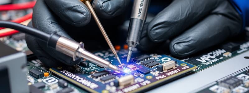
Soldering
Soldering
Signup and view all the flashcards
Solder
Solder
Signup and view all the flashcards
Brazing
Brazing
Signup and view all the flashcards
Welding
Welding
Signup and view all the flashcards
Electronic Assembly
Electronic Assembly
Signup and view all the flashcards
Printed Circuit Board (PCB)
Printed Circuit Board (PCB)
Signup and view all the flashcards
Soldering Process
Soldering Process
Signup and view all the flashcards
Solder Paste
Solder Paste
Signup and view all the flashcards
Stencil Printing
Stencil Printing
Signup and view all the flashcards
Solder Paste Stencil
Solder Paste Stencil
Signup and view all the flashcards
Reflow Soldering
Reflow Soldering
Signup and view all the flashcards
Reflow Oven/Furnace
Reflow Oven/Furnace
Signup and view all the flashcards
Temperature Profile
Temperature Profile
Signup and view all the flashcards
Mass Soldering
Mass Soldering
Signup and view all the flashcards
Flux
Flux
Signup and view all the flashcards
What is Moore's Law?
What is Moore's Law?
Signup and view all the flashcards
What is Rent's Rule?
What is Rent's Rule?
Signup and view all the flashcards
What is the trend in microprocessor pin count?
What is the trend in microprocessor pin count?
Signup and view all the flashcards
What are interconnection hierarchies?
What are interconnection hierarchies?
Signup and view all the flashcards
What is the first microprocessor?
What is the first microprocessor?
Signup and view all the flashcards
What is minimum feature size on a microprocessor?
What is minimum feature size on a microprocessor?
Signup and view all the flashcards
What are bond pads on a microprocessor?
What are bond pads on a microprocessor?
Signup and view all the flashcards
What was the minimum feature size of the first microprocessor?
What was the minimum feature size of the first microprocessor?
Signup and view all the flashcards
Wire bonding
Wire bonding
Signup and view all the flashcards
Decapping
Decapping
Signup and view all the flashcards
PCB
PCB
Signup and view all the flashcards
Level one interconnection
Level one interconnection
Signup and view all the flashcards
Wirebond
Wirebond
Signup and view all the flashcards
Flip Chip
Flip Chip
Signup and view all the flashcards
Underfill
Underfill
Signup and view all the flashcards
Study Notes
Electronics Manufacturing
- Electronics manufacturing is a large, complex, and rapidly evolving industry
- Key processes include lithography, drilling, etching, and plating
- Interconnection requirements/hierarchies are crucial for complex products
- Component types and their manufacture are essential factors in electronics assembly
- PCB manufacturing processes are critical to production
- Soldering processes connect components to PCBs
- Contamination control, yield, and testing are crucial to high-quality products
Introduction to Electronics Manufacturing
- Electronic products cover a wide range of applications, including consumer, transport, medical, military, industrial, and telecommunications sectors
- Consumer electronics encompass various devices, such as smartphones, TVs, and gaming consoles
- Other examples of appliances are washing machines and cam timers
- The transport sector uses electronics in aircraft, cars, and other vehicles, with controls for features like braking systems, and electronic throttle control
- Telecommunications use electronics for data centers and network infrastructure, with specialized applications like fibre optics
Technology Trends
- The rapid evolution of electronics is driven by technology trends, emphasizing both speed and functional requirements
- Comparing electronics to other technologies reveals significant advancements, like faster speeds, and smaller forms
- These historical trends show radical changes in speed, size and cost of items, and were made possible thanks to the development of valves to transistors, and the invention of integrated circuits
Interconnection Requirements/Hierarchies
- Interconnection hierarchies are crucial in electronics manufacturing, as they connect components in layers
- Level 1 interconnections: connect components to the outside world
- Level 2 interconnections: connect these components to printed circuit boards (PCBs)
Component Types and Their Manufacture
- There are two main categories of electrically-based components: Passive and Active
- Passive components include resistors, capacitors, and inductors
- Active components include diodes, transistors, and integrated circuits (ICs)
- Various physical forms of components exist, based on mounting method
PCB Manufacturing Processes
- PCB materials are essential to production, particularly substrates and conductors, including copper foil
- Lithographic processes (like imaging, etching, and plating) are crucial for creating the necessary circuits on PCBs
- Drilling prepares holes for the electrical connections
- The manufacturing of single-sided, double-sided plated-through-hole(PTH) and multilayer PCBs have differing steps, and need varying levels of accuracy and complexity
- There are alternative hole-formation processes, such as punching, moulding, and laser drilling
- Routing and cutting out PCBs is another step
- Exposure methods for photoresist include contact, proximity and projection methods
- Contrast in photoresist determines response to varying exposures
Soldering Processes
- Solder alloys are commonly used for joins, and include elements like tin, lead, copper, and others
- Intermetallics must be present in good solder joints, but need to be of a controlled thickness
- Forms of solder include wire, paste, and bulk
- Soldering processes encompass hand soldering, reflow soldering, and mass soldering
- Various considerations are essential in safe operating areas, such as temperature thresholds and durations during soldering, flux activity, and the use of protective measures
Contamination Control, Yield, and Testing
- Yield calculations consider the exponential distribution of defects in each step of electronics manufacturing
- Cleanliness in electronics manufacturing is crucial for preventing defects
- Cleanrooms are designed to minimize contamination, with features like clean materials and air systems
- Inspection and tests are done regularly and across all production phases to ensure high quality
Other Relevant Topics
- Moore's Law is a key concept, referring to the steady increase in the number of transistors in a chip every two years
- Metal Cutting Precision and SKF are examples of factors that have greatly changed over time, and thus reflect the increasing importance in high precision manufacturing
- Different technologies result from innovations and advances in electronics, like better memory, and improved circuit design.
- Examples include a typical desktop computer assembly in 1999 and a comparison of different components and how they have changed since then
Studying That Suits You
Use AI to generate personalized quizzes and flashcards to suit your learning preferences.


