Podcast
Questions and Answers
What is the primary function of the reverse mask in the semi-additive process?
What is the primary function of the reverse mask in the semi-additive process?
- To expose parts of the substrate for copper plating (correct)
- To insulate the areas not needing copper
- To coat the entire board in copper
- To etch away unwanted copper from the board
Which chemical is commonly used for chemical etching in PCB fabrication?
Which chemical is commonly used for chemical etching in PCB fabrication?
- Hydrochloric acid
- Sodium hydroxide
- Acetic acid
- Ammonium persulfate (correct)
What is one significant advantage of the additive method over the subtractive method in PCB manufacturing?
What is one significant advantage of the additive method over the subtractive method in PCB manufacturing?
- It requires more intricate drilling techniques.
- It produces more waste material.
- It creates a thicker copper layer.
- It removes less copper. (correct)
In PCB milling, what is primarily milled away from the substrate?
In PCB milling, what is primarily milled away from the substrate?
What is typically used for drilling holes through a PCB?
What is typically used for drilling holes through a PCB?
During the semi-additive process, what is applied to create conductive vias in multi-layer boards?
During the semi-additive process, what is applied to create conductive vias in multi-layer boards?
Which process involves vaporizing paint to define areas where etching will occur?
Which process involves vaporizing paint to define areas where etching will occur?
What typically happens to the bare copper areas during the chemical etching process?
What typically happens to the bare copper areas during the chemical etching process?
Which material is most commonly used for the base of a printed circuit board?
Which material is most commonly used for the base of a printed circuit board?
What technology is characterized by components being soldered directly onto the surface of the PCB?
What technology is characterized by components being soldered directly onto the surface of the PCB?
Which of the following describes the main types of PCBs?
Which of the following describes the main types of PCBs?
What does FR in FR-4 denote regarding PCB materials?
What does FR in FR-4 denote regarding PCB materials?
Who first developed the printed circuit board?
Who first developed the printed circuit board?
Which of the following is NOT a characteristic of through-hole technology?
Which of the following is NOT a characteristic of through-hole technology?
Which process was used for PCB design before computerized methods became common?
Which process was used for PCB design before computerized methods became common?
What type of PCB uses high-temperature plastic as its substrate?
What type of PCB uses high-temperature plastic as its substrate?
What is the primary reason for recommending coated tungsten carbide drill bits for PCB manufacturing?
What is the primary reason for recommending coated tungsten carbide drill bits for PCB manufacturing?
What file type is used to control the placement of drill bits during PCB drilling?
What file type is used to control the placement of drill bits during PCB drilling?
What are micro vias, and how are they typically created?
What are micro vias, and how are they typically created?
Which type of via connects an internal copper layer to an outer layer?
Which type of via connects an internal copper layer to an outer layer?
What purpose does the solder mask serve after PCBs are etched?
What purpose does the solder mask serve after PCBs are etched?
What is the primary method of making conductive holes in PCBs?
What is the primary method of making conductive holes in PCBs?
What treatment is applied to bare copper to prevent surface oxidation?
What treatment is applied to bare copper to prevent surface oxidation?
How do buried vias differ from blind vias?
How do buried vias differ from blind vias?
What is the primary function of panelization in PCB manufacturing?
What is the primary function of panelization in PCB manufacturing?
Which method is NOT typically used in the depaneling process of PCBs?
Which method is NOT typically used in the depaneling process of PCBs?
Which function is associated with the PCB CAM system?
Which function is associated with the PCB CAM system?
What is the purpose of silk screen printing in the copper patterning process?
What is the purpose of silk screen printing in the copper patterning process?
What does the term 'depaneling' refer to in PCB manufacturing?
What does the term 'depaneling' refer to in PCB manufacturing?
Which of the following statements about bare board manufacturing panels is true?
Which of the following statements about bare board manufacturing panels is true?
What role does subsequent etching play in copper patterning?
What role does subsequent etching play in copper patterning?
Which technique is utilized for high-resolution requirements in photoengraving?
Which technique is utilized for high-resolution requirements in photoengraving?
Flashcards
Printed Circuit Board (PCB)
Printed Circuit Board (PCB)
A non-conductive substrate that mechanically supports and electrically connects electronic components using etched copper traces.
PCB Assembly (PCBA)
PCB Assembly (PCBA)
A PCB with electronic components soldered onto it.
Single-sided PCB
Single-sided PCB
A PCB with components and traces on only one side.
Double-sided PCB
Double-sided PCB
Signup and view all the flashcards
Multilayer PCB
Multilayer PCB
Signup and view all the flashcards
Copper Foil
Copper Foil
Signup and view all the flashcards
Copper Plating
Copper Plating
Signup and view all the flashcards
Solder Mask
Solder Mask
Signup and view all the flashcards
Through-hole Technology
Through-hole Technology
Signup and view all the flashcards
Surface Mount Technology
Surface Mount Technology
Signup and view all the flashcards
FR-4
FR-4
Signup and view all the flashcards
PCB CAM
PCB CAM
Signup and view all the flashcards
Panelization
Panelization
Signup and view all the flashcards
Assembly panel
Assembly panel
Signup and view all the flashcards
Bare board manufacturing panel
Bare board manufacturing panel
Signup and view all the flashcards
Depaneling
Depaneling
Signup and view all the flashcards
Copper patterning
Copper patterning
Signup and view all the flashcards
Silk screen printing
Silk screen printing
Signup and view all the flashcards
Photoengraving
Photoengraving
Signup and view all the flashcards
PCB Milling
PCB Milling
Signup and view all the flashcards
Laser Resist Ablation
Laser Resist Ablation
Signup and view all the flashcards
Additive PCB Process
Additive PCB Process
Signup and view all the flashcards
Semi-Additive PCB Process
Semi-Additive PCB Process
Signup and view all the flashcards
Chemical Etching
Chemical Etching
Signup and view all the flashcards
PTH (plated-through holes)
PTH (plated-through holes)
Signup and view all the flashcards
Drilling
Drilling
Signup and view all the flashcards
Coated tungsten carbide drill bits
Coated tungsten carbide drill bits
Signup and view all the flashcards
High-speed-steel drill bits (for PCB drilling)
High-speed-steel drill bits (for PCB drilling)
Signup and view all the flashcards
Automated drilling machines (PCB)
Automated drilling machines (PCB)
Signup and view all the flashcards
Drill file (or NCD/Excellon file)
Drill file (or NCD/Excellon file)
Signup and view all the flashcards
Conductive holes (PCB)
Conductive holes (PCB)
Signup and view all the flashcards
Vias (PCB)
Vias (PCB)
Signup and view all the flashcards
Laser-drilled vias (PCB)
Laser-drilled vias (PCB)
Signup and view all the flashcards
Micro vias (PCB)
Micro vias (PCB)
Signup and view all the flashcards
Blind vias (PCB)
Blind vias (PCB)
Signup and view all the flashcards
Buried vias (PCB)
Buried vias (PCB)
Signup and view all the flashcards
PCB plating (solder, tin, or gold)
PCB plating (solder, tin, or gold)
Signup and view all the flashcards
Solder mask (PCB)
Solder mask (PCB)
Signup and view all the flashcards
Matte solder (PCB)
Matte solder (PCB)
Signup and view all the flashcards
Study Notes
PCB Designing
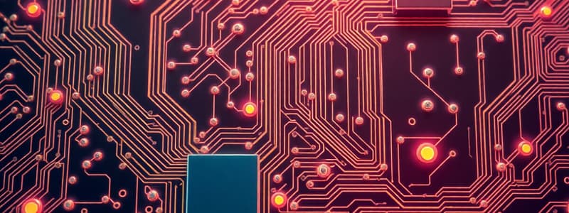
- Printed Circuit Board (PCB): A non-conductive substrate mechanically supporting and electrically connecting electronic components. Components are connected using etched tracks, pads, and other features on a laminated copper sheet.
- Printed Circuit Board Assembly (PCBA): A PCB populated with electronic components.
- History: First developed by Australian engineer Paul Eisler. Earlier point-to-point wiring and later wire wrapping preceded PCBs.
- Types of PCBs:
- Single-sided
- Double-sided
- Multilayer
- PCB Materials:
- Copper-clad fiberglass (or thin copper sheets)
- Copper foil
- Copper plating
- Solder flow
- Solder mask
- Traces
- Slots and cutouts
- Through-Hole Technology: Early PCBs used this method to install components. Leads pass through holes in one side of the board and are soldered to traces on the other side. Boards can be single- or double-sided.
- Surface Mount Technology (SMT): Emerged in the 1960s. Components with small metal tabs or end caps are directly soldered to the PCB surface.
- PCB Base Material: Fiberglass, specifically FR-4. FR-4 is a flame-retardant composite material.
- PCB Design Equipment (Early Days): Design and layout was done manually using tape placed on translucent film, then photographically reduced for manufacturing.
- Modern PCB Design Equipment: Computerized design, PCB CAM (Computer-Aided Manufacturing) systems, and software packages for improved efficiency and more features (like simulations and complex routing).
- PCB CAM Functions:
- Input of fabrication data.
- Data verification (and potentially Design for Manufacturing (DFM).
- Compensation for manufacturing process deviations (e.g., scaling).
- Panelization: Grouping multiple PCBs for manufacturing onto a larger panel. Can use single design or mix several designs on a single panel.
- Output of digital tools (copper patterns, solder mask, legend, drill files, and other data needed for production).
- Depaneling: Breaking the panel into individual PCBs. The process is often assisted with lines or cuts in the panel, and now often done by lasers for better results.
- Copper Patterning: Reproducing the copper pattern using either silk screen printing, photoengraving (using UV-sensitive resists), or other direct imaging techniques, to create the desired copper layout, removing unwanted copper.
- PCB Milling: A mechanical method to remove copper.
- Laser Resist Ablation: A process for removing unwanted copper using a laser and a coating for resistance in certain areas.
- Subtractive, Additive, and Semi-Additive Processes:
- Subtractive method: Removing copper from an entire copper-coated board.
- Additive method: Adding the desired copper pattern on a plain substrate.
- Semi-additive: The board starts with a thin copper layer and a reverse mask to deposit more copper to the desired areas.
- Chemical Etching: Using chemical solutions (like ammonium persulfate or ferric chloride) to remove copper from a PCB. Crucial for Plated-Through-Holes (PTH).
- Drilling: Using small drill bits (often made of tungsten carbide) to create holes in the PCB.
- Vias: Small holes for connecting board layers, or for passing components and signals between layers. Can also have micro vias.
- Blind Vias: Connecting an internal layer to an outer layer without passing through the entire board.
- Buried Vias: Connecting layers on a PCB but do not pass through the outer layers.
- Plating and Coating: Applying solder, tin, gold, or nickel to the copper to act as a physical and/or chemical coating/resistance to allow copper etch/removal.
- Legend Printing: Using screen printing, liquid photo imaging, or ink-jet printing to print labels and other information onto the board.
- Final Steps: Testing, soldering, packaging, and protection after the PCB assembly is completed.
- Advantages of PCBs: Fixed components, minimal short circuit/wiring concerns, inexpensive for mass production, perfect for reproduction.
- Disadvantages of PCBs: Not easily repairable once damaged, potential environmental impact, difficult to update designs, and limited to specific circuits.
Studying That Suits You
Use AI to generate personalized quizzes and flashcards to suit your learning preferences.


