Podcast
Questions and Answers
What geometric shape do gold nanocrystals larger than 0.8 nm typically exhibit?
What geometric shape do gold nanocrystals larger than 0.8 nm typically exhibit?
- Truncated octahedron or cubooctahedron (correct)
- Cubic or hexagonal prism
- Irregular or amorphous
- Spherical or ellipsoidal
What percentage of surface atoms on a 1-2 nm Au cluster are likely to be found on edges or corners?
What percentage of surface atoms on a 1-2 nm Au cluster are likely to be found on edges or corners?
- 20%
- 45% (correct)
- 60%
- 33%
Which aspect of the thiol layer in nanoparticles suggests that it may not be densely packed?
Which aspect of the thiol layer in nanoparticles suggests that it may not be densely packed?
- The outer part of the thiol layer appears loosely packed (correct)
- High variation in particle size
- Lack of surface defects
- The presence of multiple reaction products
What is the effect of the increasing density of n-alkanethiols as they move away from the surface of a nanoparticle?
What is the effect of the increasing density of n-alkanethiols as they move away from the surface of a nanoparticle?
Why should caution be taken while using geometric and computational models for gold nanoparticles?
Why should caution be taken while using geometric and computational models for gold nanoparticles?
How does the area available to each chain on a nanoparticle compare with that on a perfectly flat single-crystal 2-D Au(111) surface?
How does the area available to each chain on a nanoparticle compare with that on a perfectly flat single-crystal 2-D Au(111) surface?
Which feature contributes to a nanoparticle coated with a well-packed self-assembled monolayer (SAM)?
Which feature contributes to a nanoparticle coated with a well-packed self-assembled monolayer (SAM)?
What characteristic of the gold cluster affects its interactions with alkanethiolate chains?
What characteristic of the gold cluster affects its interactions with alkanethiolate chains?
What type of structure is primarily formed when using a 100 mM thiol solution in µCP?
What type of structure is primarily formed when using a 100 mM thiol solution in µCP?
Which factor does NOT significantly influence the type of structures produced in SAMs according to the content?
Which factor does NOT significantly influence the type of structures produced in SAMs according to the content?
What is a likely consequence of low mass coverage phases during the µCP process?
What is a likely consequence of low mass coverage phases during the µCP process?
Which structures are suggested to be formed when the specific proportion of thiol concentration is optimized to 1 mM for 18 hours?
Which structures are suggested to be formed when the specific proportion of thiol concentration is optimized to 1 mM for 18 hours?
What characteristic size is established for lateral dimensions when nanostructures are formed via µCP?
What characteristic size is established for lateral dimensions when nanostructures are formed via µCP?
Which aspect significantly contributes to the challenges of fabricating small structures using µCP?
Which aspect significantly contributes to the challenges of fabricating small structures using µCP?
Which type of packing arrangement is associated with striped phases during printed patterns?
Which type of packing arrangement is associated with striped phases during printed patterns?
What primarily defines the resolution limits in µCP according to the content?
What primarily defines the resolution limits in µCP according to the content?
What is the primary advantage of using poly(dimethylsiloxane) (PDMS) for stamping in microcontact printing?
What is the primary advantage of using poly(dimethylsiloxane) (PDMS) for stamping in microcontact printing?
What limitation does the size of molecular precursors for cross-linking impose on microcontact printing?
What limitation does the size of molecular precursors for cross-linking impose on microcontact printing?
Which technique is specifically used to create a self-assembled monolayer on exposed areas after removing the stamp?
Which technique is specifically used to create a self-assembled monolayer on exposed areas after removing the stamp?
Which of the following is a key characteristic of Sylgard 184 that makes it advantageous for creating stamps?
Which of the following is a key characteristic of Sylgard 184 that makes it advantageous for creating stamps?
What range of feature sizes can be replicated using techniques involving PDMS stamps?
What range of feature sizes can be replicated using techniques involving PDMS stamps?
What is the typical in-plane dimension range achievable by microcontact printing?
What is the typical in-plane dimension range achievable by microcontact printing?
Which mass transport mechanism is crucial for the formation of self-assembled monolayers (SAM) during the stamping process?
Which mass transport mechanism is crucial for the formation of self-assembled monolayers (SAM) during the stamping process?
What is the significance of using a flat slab of PDMS soaked in thiols during stamping?
What is the significance of using a flat slab of PDMS soaked in thiols during stamping?
What primarily impacts the grafting density of self-assembled monolayers (SAMs) formed during µCP?
What primarily impacts the grafting density of self-assembled monolayers (SAMs) formed during µCP?
Which condition is likely to result in the least grafting density of PDMS during the stamping process?
Which condition is likely to result in the least grafting density of PDMS during the stamping process?
Which structural characteristic correlates with higher grafting density in SAMs?
Which structural characteristic correlates with higher grafting density in SAMs?
What factor did NOT significantly affect the grafting density of PDMS during µCP?
What factor did NOT significantly affect the grafting density of PDMS during µCP?
Which effect is likely to enhance the grafting density of SAMs formed from high concentrations of thiol?
Which effect is likely to enhance the grafting density of SAMs formed from high concentrations of thiol?
Which circumstance could lead to contamination affecting grafting density in PDMS deposits?
Which circumstance could lead to contamination affecting grafting density in PDMS deposits?
Which phenomenon indicates a successful high grafting density in a printing process?
Which phenomenon indicates a successful high grafting density in a printing process?
What is a potential drawback of achieving increased grafting density in SAMs?
What is a potential drawback of achieving increased grafting density in SAMs?
What effect does the molecular precursor size have on the minimum feature dimensions in microcontact printing?
What effect does the molecular precursor size have on the minimum feature dimensions in microcontact printing?
How does the surface energy of PDMS influence the pattern transfer during microcontact printing?
How does the surface energy of PDMS influence the pattern transfer during microcontact printing?
Which factor primarily determines the distances between replicated features in microcontact printing?
Which factor primarily determines the distances between replicated features in microcontact printing?
What can be inferred about the mechanical properties of PDMS that make it suitable for stamping applications?
What can be inferred about the mechanical properties of PDMS that make it suitable for stamping applications?
Which of the following describes the primary limitation of using Sylgard 184 in microcontact printing?
Which of the following describes the primary limitation of using Sylgard 184 in microcontact printing?
What characteristic of thiol solutions is crucial for creating self-assembled monolayers after stamp removal?
What characteristic of thiol solutions is crucial for creating self-assembled monolayers after stamp removal?
In what way does the 'contact inking' technique improve microcontact printing outcomes?
In what way does the 'contact inking' technique improve microcontact printing outcomes?
Which property of the thiols used in microcontact printing contributes to the creation of dense self-assembled monolayers?
Which property of the thiols used in microcontact printing contributes to the creation of dense self-assembled monolayers?
What does the term 'grafting density' refer to in the context of nanoparticle coatings?
What does the term 'grafting density' refer to in the context of nanoparticle coatings?
How does increasing the grafting density of n-alkanethiols on gold nanoparticles affect their properties?
How does increasing the grafting density of n-alkanethiols on gold nanoparticles affect their properties?
What consequence does a low grafting density have on the stability of gold nanoparticles?
What consequence does a low grafting density have on the stability of gold nanoparticles?
Which factor is NOT a consequence of increased packing density of thiol chains on nanoparticles?
Which factor is NOT a consequence of increased packing density of thiol chains on nanoparticles?
What effect does the geometry of nanoparticles have on grafting density?
What effect does the geometry of nanoparticles have on grafting density?
Which of the following statements best describes the relationship between surface construction and grafting density?
Which of the following statements best describes the relationship between surface construction and grafting density?
In the context of self-assembled monolayers (SAMs), what outcome is associated with lower grafting densities?
In the context of self-assembled monolayers (SAMs), what outcome is associated with lower grafting densities?
What primarily dictates the coverage of thiol chains over a nanoparticle surface?
What primarily dictates the coverage of thiol chains over a nanoparticle surface?
Study Notes
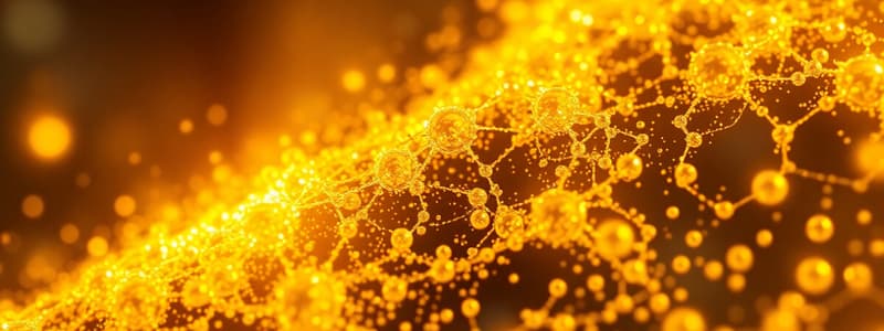
Gold Nanocrystals
- Gold nanocrystals larger than 0.8 nm often have a truncated octahedral or cubooctahedral shape.
- These structures are characterized by eight {111} faces truncated by six smaller {100} faces.
- The surface of these nanocrystals has a higher percentage of regions where the construction changes (corners and edges) compared to planar substrates.
- Approximately 45% of surface atoms on a 1-2 nm Au cluster are located on edges or corners.
Thermal Gravimetric Analysis
- Thermal gravimetric analysis (TGA) has shown that small nanoparticles (60% coverage) have a higher coverage of thiols than a perfectly flat Au(111) surface (33%).
- This high coverage is attributed to the occupancy of alternative binding sites (edges and corners) and can be modeled geometrically and computationally.
- However, the exact mixture of reaction products from nanocluster preparations has not been fully characterized.
Microcontact Printing (µCP)
- µCP is a technique used for creating patterned self-assembled monolayers (SAMs) on surfaces.
- µCP utilizes a stamp with raised regions that are inked with a solution of thiols.
- The stamp is then pressed against a substrate, transferring the thiols to the surface.
- The technique is used for producing patterns on areas ranging from 0.1-100 cm2 with in-plane dimensions of ∼50 nm to 1000 µm.
- One advantage of µCP is the ability to generate a second SAM on remaining bare regions of the surface by either immersion or application of a second stamp.
Stamp Composition in µCP
- Poly(dimethylsiloxane) (PDMS) is the most commonly used material for µCP stamps.
- PDMS is nontoxic, commercially available, elastomeric, and has a low surface energy.
- It is well-suited for forming stamps because it can replicate features on the order of 0.3 µm without significant distortions.
- Sylgard 184 is a common formulation of PDMS used for forming stamps due to its commercial availability, affordability, and ease of use.
Limitation of µCP
- µCP can create features as small as 50 nm, but the fabrication of such small structures remains a challenge.
- Two key factors limiting resolution are lateral diffusion of molecules and distortions of the stamp.
- Lateral diffusion of ink molecules broadens the printed features.
- The smallest features replicated by molding to date are approximately 1.5 nm in the direction normal to the surface of the stamp.
SAMs Formed by µCP
- SAMs formed by µCP on Au(111) exhibit a mixture of structures including disordered regions, striped phases with p × x3 packing arrangements (p = 3.5, 4, 8, 5), and dense (x3 × x3)-R30° structures with a c4 × 2 superlattice.
- The concentration of thiol used for printing influences the percentage of each type of structure and the domain sizes.
- The contact time (0.3-30 s) appears to have a small effect on the resulting structures.
Contamination in µCP
- Some studies have reported trace contaminants from PDMS remaining on the surface after printing.
- The effect of these contaminants on the structure and properties of the SAMs is not fully understood.
- The composition of the prepolymer, curing time, ratio of components, and extraction procedures may affect the degree of contamination.
Gold Nanocrystal Shape and Size
- Gold nanocrystals larger than 0.8 nm have a truncated octahedral or cubooctahedral shape, with eight {111} faces truncated by six smaller {100} faces.
- The percentage of surface atoms on the corners and edges of the truncated octahedron is higher on nanocrystals compared to planar substrates.
- About 45% of surface atoms on a 1-2 nm Au cluster are located on the edges or corners.
Thiol Passivation of Gold Nanocrystals
- Small nanoparticles have a higher density of thiol molecules compared to flat gold surfaces.
- The density of thiol chains decreases as the distance from the surface of the nanocrystal core increases.
- Molecular dynamics simulations show that the outer part of the thiol layer on Au140 nanoclusters is loosely packed.
µCP Fabrication
- Microcontact printing (µCP) uses a stamp to transfer a pattern of molecules onto a surface.
- The most common material for the stamp is poly(dimethylsiloxane) (PDMS).
- PDMS is a nontoxic, elastomeric silicone rubber with low surface energy.
- Fabrication methods for µCP masters include photolithography, micromachining, and anisotropic chemical etching.
µCP Resolution
- The size of the molecular precursors for the cross-linked polymer in the stamp determines the minimum dimensions of the features that can be replicated.
- The smallest features replicated by molding are approximately 1.5nm, which corresponds to the direction normal to the surface of the stamp.
Self-Assembled Monolayers (SAMs) Formed by µCP
- SAMs formed by µCP on gold surfaces often exhibit a mixture of structures, including disordered regions, striped phases, and dense structures.
- The concentration of thiol used for printing, rather than contact time, primarily influences the percentage and domain size of each type of structure in the SAM.
Contamination Concerns in µCP
- Trace contaminants from PDMS can be left on the surface after printing.
- The degree of contamination depends on factors like the composition of the prepolymer, curing time, and procedures used to extract low molecular weight siloxanes.
Limitations of µCP for Nanostructure Fabrication
- µCP can be used to form nanostructures with lateral dimensions as small as 50 nm.
- Lateral diffusion of molecules and distortions in the stamp are key factors limiting the resolution of µCP.
- Lateral broadening of the printed features results from diffusion through the gas phase or surface-mediated processes.
Studying That Suits You
Use AI to generate personalized quizzes and flashcards to suit your learning preferences.
Description
Explore the fascinating world of gold nanocrystals, their unique shapes, and the impact of surface atom distribution on their properties. This quiz also delves into thermal gravimetric analysis and microcontact printing techniques used in nanofabrication. Test your knowledge on these advanced topics in nanotechnology.


