Podcast
Questions and Answers
What is the primary function of a transistor?
What is the primary function of a transistor?
- To directly amplify power without external input.
- To regulate current or amplify an input signal. (correct)
- To store electrical energy for later use.
- To convert AC current to DC current.
According to general physics principles, why is the term 'amplification' used to describe a transistor's function considered misleading?
According to general physics principles, why is the term 'amplification' used to describe a transistor's function considered misleading?
- Because transistors create energy from nothing, violating the laws of thermodynamics.
- Because transistors actually control energy from a power supply, rather than create it. (correct)
- Because amplification is a property exclusive to vacuum tubes, not semiconductors.
- Because transistors only switch signals, they do not amplify them.
How are Bipolar Junction Transistors (BJTs) generally categorized?
How are Bipolar Junction Transistors (BJTs) generally categorized?
- As power-controlled devices.
- As voltage-controlled devices.
- As resistance-controlled devices.
- As current-controlled devices. (correct)
Which characteristic primarily defines Field-Effect Transistors (FETs)?
Which characteristic primarily defines Field-Effect Transistors (FETs)?
Who is credited with the invention of the transistor?
Who is credited with the invention of the transistor?
In what year was the invention of the transistor announced?
In what year was the invention of the transistor announced?
What is the dominant type of transistor in modern integrated circuits?
What is the dominant type of transistor in modern integrated circuits?
According to Moore's Law, what trend did Gordon Moore predict?
According to Moore's Law, what trend did Gordon Moore predict?
What are the three terminals of a Bipolar Junction Transistor (BJT)?
What are the three terminals of a Bipolar Junction Transistor (BJT)?
In an NPN transistor, what is the material composition of the base region?
In an NPN transistor, what is the material composition of the base region?
Which of the following is true regarding the base of a BJT?
Which of the following is true regarding the base of a BJT?
How are the collector and emitter typically connected in a BJT circuit?
How are the collector and emitter typically connected in a BJT circuit?
What serves as a mnemonic for the circuit symbol of an NPN transistor?
What serves as a mnemonic for the circuit symbol of an NPN transistor?
What are the three terminals in a Field Effect Transistor (FET)?
What are the three terminals in a Field Effect Transistor (FET)?
What is the key feature that all FETs share?
What is the key feature that all FETs share?
What is the primary difference between Junction FETs (JFETs) and MOSFETs?
What is the primary difference between Junction FETs (JFETs) and MOSFETs?
What operational mode is exclusive to JFETs?
What operational mode is exclusive to JFETs?
In an N-channel JFET, what happens when a reverse bias voltage is applied to the gate terminal?
In an N-channel JFET, what happens when a reverse bias voltage is applied to the gate terminal?
What material typically insulates the gate from the channel in a MOSFET?
What material typically insulates the gate from the channel in a MOSFET?
In basic transistor operation, what occurs when a small current is applied to the base terminal (B) of a BJT?
In basic transistor operation, what occurs when a small current is applied to the base terminal (B) of a BJT?
If a BJT has an amplification of 200 and a base current of 2mA is applied, what approximate current will flow into the collector before reaching maximum rated values?
If a BJT has an amplification of 200 and a base current of 2mA is applied, what approximate current will flow into the collector before reaching maximum rated values?
Why is forward bias of the Base Emitter junction required to turn a BJT 'on'?
Why is forward bias of the Base Emitter junction required to turn a BJT 'on'?
A PNP transistor circuit has a positive voltage applied to the collector with respect to the emitter. What should be the polarity of the voltage applied to the base with respect to the emitter to properly bias the transistor?
A PNP transistor circuit has a positive voltage applied to the collector with respect to the emitter. What should be the polarity of the voltage applied to the base with respect to the emitter to properly bias the transistor?
In a common-emitter amplifier configuration using an NPN BJT, as the base current increases, what is the effect on the collector-emitter voltage ($V_{CE}$)?
In a common-emitter amplifier configuration using an NPN BJT, as the base current increases, what is the effect on the collector-emitter voltage ($V_{CE}$)?
Flashcards
What is a Transistor?
What is a Transistor?
A three-terminal semiconductor device used to regulate current or amplify an input signal into a greater output signal, also used to switch electronic signals.
What is a Transistor's Amplification?
What is a Transistor's Amplification?
A control device where a small amount of input current/voltage controls a larger amount of power supply current/voltage, giving the impression of amplification.
What are the two basic categories of transistors?
What are the two basic categories of transistors?
Bipolar Junction Transistor (BJT) and Field-Effect Transistor (FET).
What is a BJT Transistor?
What is a BJT Transistor?
Signup and view all the flashcards
What is a FET Transistor?
What is a FET Transistor?
Signup and view all the flashcards
What are the three terminals of a BJT?
What are the three terminals of a BJT?
Signup and view all the flashcards
What is the Base of a BJT?
What is the Base of a BJT?
Signup and view all the flashcards
What is the Collector of a BJT?
What is the Collector of a BJT?
Signup and view all the flashcards
What is the Emitter of a BJT?
What is the Emitter of a BJT?
Signup and view all the flashcards
What are NPN and PNP?
What are NPN and PNP?
Signup and view all the flashcards
What are the three terminals of a FET?
What are the three terminals of a FET?
Signup and view all the flashcards
What do FETs have in common?
What do FETs have in common?
Signup and view all the flashcards
What are Junction FETs (JFETs)?
What are Junction FETs (JFETs)?
Signup and view all the flashcards
What are MOSFETs?
What are MOSFETs?
Signup and view all the flashcards
What are the operating modes of MOSFETs and JFETs?
What are the operating modes of MOSFETs and JFETs?
Signup and view all the flashcards
What is enhancement mode?
What is enhancement mode?
Signup and view all the flashcards
What is a Junction FET (JFET)?
What is a Junction FET (JFET)?
Signup and view all the flashcards
How N-Channel JFETs work?
How N-Channel JFETs work?
Signup and view all the flashcards
Are the letters (B, C and E or D, G and S) a requirement?
Are the letters (B, C and E or D, G and S) a requirement?
Signup and view all the flashcards
What happens in basic transistor operation?
What happens in basic transistor operation?
Signup and view all the flashcards
What are BJTs terminals?
What are BJTs terminals?
Signup and view all the flashcards
What are amplification functions?
What are amplification functions?
Signup and view all the flashcards
What does the increased collector/emitter current result?
What does the increased collector/emitter current result?
Signup and view all the flashcards
What is Base/Emitter junction?
What is Base/Emitter junction?
Signup and view all the flashcards
When will the BJT turn on? (being current controlled)
When will the BJT turn on? (being current controlled)
Signup and view all the flashcards
Study Notes
The Transistor
- A three-terminal semiconductor device is commonly called a transistor
- Transistors regulate current, amplify an input signal into a greater output signal, and switch electronic signals
- A transistor cannot amplify by itself
- Amplification is increasing the amplitude of an electrical signal or oscillation
- Transistors act as control devices
Transistor Categories
- Bipolar Junction Transistor (BJT)
- Field-Effect Transistor (FET)
- The construction and theory of operation differ greatly between the two
- BJTs are categorized as current-controlled devices
- FETs are categorized as voltage-controlled devices
History of Transistors
- American physicists John Bardeen, Walter H. Brattain, and William Shockley invented the transistor
- It was announced by Bell Telephone Laboratories in 1948
- The invention was part of a post-war effort to replace vacuum tubes with solid-state devices
- The first transistor was created in 1947
- Most transistors today are built as part of integrated circuits
- Transistors are in nearly all electronic devices
- BJT was the most common transistor between the 1950s and 1960s
- The BJT was the first solid-state amplifier element, starting the solid-state electronics revolution
- Since the 1970s, MOSFETs have dominated due to advantages in integrated circuits
- MOSFETs make up 99.9% of all transistors on the market
- The average computer CPU has over 5 billion MOSFETs
- The average Graphics Processing Unit (GPU) contains approximately 30-60 billion MOSFETs
- In 1965, Intel's co-founder Gordon Moore predicted that microchip performance and the number of transistors in a microchip would double every two years - know as Moore's Law
- As of 2021, microprocessors were manufactured with transistors less than 5 nanometers wide
- A silicon atom measures about 0.2 nanometers wide
Bipolar Junction Transistors
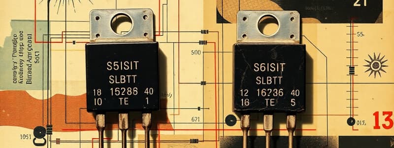
- BJTs are three-terminal devices
- The terminals are Base, Collector, and Emitter
- The collector and emitter are normally connected to the power supply through other components
- The base is normally in the input signal to be amplified
- The base is a very narrow region in the center
- The collector is a relatively large weakly doped region
- The collector's size reduces resistance and allows greater heat dissipation
- The emitter is a strongly doped region of the same type as the collector
- BJTs are classified as either NPN or PNP based on the arrangement of their N and P materials
- An NPN transistor is formed by introducing a thin region of P-type material between two regions of N-type material
- Semiconductor orientation flipped forms a PNP transistor, where a thin region of N-type material is introduced between two regions of P-type material
- BJT has two PN junctions, one between the emitter and base, the other between the collector and base
- The two junctions share one section of semiconductor material
- Transistors consist of three elements
- A transistor is similar to two back-to-back diodes (two PN junctions)
- The operation depends on the interaction of depletion regions in the narrow base, not similar to two diodes
Transistor Mnemonics
- NPN - Never Points iN
- PNP - Points iN Permanently
- NPN - Arrow points out between the base and emitter
- PNP - Arrow points in towards the base from the emitter
Field Effect Transistors
- FETs come in more varieties than BJTs
- FETs are three-terminal devices, terminals are: Drain, Source, Gate
- The drain and source are normally connected to the power supply via other components
- The gate is normally the input signal to be amplified
- Field-effect transistor has only two sections of semiconductor material
- FETs current flow is controlled by an applied electric field
- The transistor part that supplies the field must be isolated from the channel
- Isolation falls into two basic categories: reverse-biased PN junctions and electrically insulating material
- Devices using reverse-biased junction isolation are:
- Junction FETs
- Jug FET (Junction Gate FET)
- JFETs
- Devices using insulating materials are:
- Metal-Oxide Semiconductor FETs
- MOSFETs
- IG FET (Insulated Gate FET)
- Most transistors in integrated circuits are MOSFETs
- Depletion type MOSFETs operate in enhancement mode and depletion mode
- JFETs only operate in depletion mode
Field effect transistor symbols
- FETs are produced as either N-channel or P-channel
- An N-channel is a FET with N-type semiconductor material operating as the channel for current flow
- The arrowhead points towards the N type material and is drawn on the Gate terminal
- An arrowhead pointing towards the channel indicates an N channel
- An arrowhead pointing away from the channel indicates a P channel
- MOSFETs have two operating types: enhancement type and depletion type
- The depletion type MOSFET can be operated in two modes:
- Enhancement Mode
- Increased gate voltage increases conductivity of the channel, allowing more current to flow
- Depletion Mode
- Transistor is "On" by default, allowing current to flow
- Applying voltage to the gate reduces conductivity, possibly turning the transistor "Off" like a switch
- Enhancement Mode
Junction FET (JFET)
- Has a channel of one semiconductor type with the other type positioned around the center channel
- Electricity flows through the "channel" from source to drain
- The gate voltage controls the depletion region around the channel
- Functions by squeezing a garden hose to restrict water flow
- Applying a reverse bias voltage to a gate terminal "squeezes" the channel, impeding or switching off electric current
- JFET is typically ON when there is no voltage between its gate and source terminals (depletion mode)
- If a potential difference of the correct polarity is applied between its gate and source terminals, the JFET becomes more resistive to current flow, and less current flows in the channel between the source and drain terminals
Metal Oxide Semiconductor FET (MOSFET)
- MOSFET is a field effect transistor
- Most MOSFETs have 3 connections
- applied Gate voltage affects current flow from the source to the drain
- The Gate is insulated from the channel by a thin film of silicon dioxide
- Channel material connects the drain and source
- Depletion type MOSFETs can be operated in either depletion or in enhancement mode
- MOSFETs can be P-channel or N-channel
- Gate voltage controls the channel's current flow
- In an N-channel MOSFET run in enhancement mode, a positive gate voltage enhances channel size, increasing current flow
- In depletion mode a higher negative voltage on the gate reduces the source to drain current
Transistor Symbols
- BJTs and FETs (JFET and MOSFET) have schematic symbols
- Each transistor has three terminals
- BJT terminals are:
- Collector (C)
- Base (B)
- Emitter (E)
- FET terminals are:
- Drain (D)
- Gate (G)
- Source (S)
- A circle is optional
- Letters are often left out of schematics
- Direction of the arrow is always from base to emitter or emitter to base
Transistor Properties
- A small signal applied between one pair of terminals can control a much larger signal at another pair of terminals
- This is called gain
- Transistors can produce a stronger output signal proportional to a weaker input signal; thus acting as an amplifier
- Transistors can also turn current on/off in a circuit as an electrically controlled switch
- BJT terminals are: Collector (C), Base (B), Emitter (E)
- FETs have different terminals, but perform same function
- With a small current applied to the base terminal (B), a larger current can flow from the collector (C) to the emitter (E)
- The flow that turns the transistor on can be much smaller than the flow that runs through the main pipe
Transistor Behaviors
- Relationship exist between base current and collector current
- Base current increase = proportional increase of collector current
- If amplification is 200 and the applied base current is 2 mA, the current flowing into the collector is 0.2 A
- This works until the maximum rated values, past the "breakdown" voltage an avalanche happens, damaging the component
- Applying voltage to the base turns a BJT on, requiring both voltage and current
- Being current-controlled, a BJT turns "on" with voltage sufficient to forward bias the Base Emitter junction and cause current
Transistor Basic Circuits
- Transistors amplify or switch electronic signals and electrical power
- NPN Transistor Biasing = Base/Emitter junction is forward biased, having a positive voltage applied to the Base with respect to the Emitter and Emitter collector voltage must reverse bias the Collector Base junction
- Adjust the base voltage until the base current is halfway between minimum and maximum
- This affects the base current flow, controlling the Collector Emitter current
- Base/Emitter increase = Collector Emitter current increases
- Base/Emitter decrease = Collector Emitter current decreases
- NPN BJT circuit with 2 V base voltage and 20 V collector/emitter voltage where voltage amplification happens by comparing base/emitter voltage change to voltage change across the collector/emitter
- Common Collector voltage (VCC) is used to produced the base bias voltage
- Increased base current results in a decrease of the output voltage
- Without voltage applied to the base, the transistor is an open circuit with no current flowing
- With a positive voltage applied (NPN Transistor), the transistor is switched on permitting current to flow between collector and emitter
Transistor Operation Graph
- The graph displays increasing levels of Base current
- The transistor with no base current is considered switched OFF
- The yellow region is unused as increasing voltage acts as a resistor that increases with voltage
- The green region exhibits an insignificant current difference at the CE voltage producing a constant current source
- The green region between 0.7 V and VCE is used for amplification
- The red region is where the collector emitter voltage is too high (above VCE), damaging the transistor
- JFETs, MOSFETs, and their variations have operating modes and regions
Studying That Suits You
Use AI to generate personalized quizzes and flashcards to suit your learning preferences.


