Podcast
Questions and Answers
What is the key role of semiconductor materials and devices in the technological landscape?
What is the key role of semiconductor materials and devices in the technological landscape?
- Supporting agricultural technologies
- Driving advancements in diverse applications (correct)
- Enhancing mechanical devices
- Improving transportation systems
Which component enables technologies like metal oxide semiconductor devices?
Which component enables technologies like metal oxide semiconductor devices?
- Microprocessors, sensors, and antennas
- Transistors, resistors, and diodes
- Semiconductors, conductors, and dielectrics (correct)
- Insulators, resistors, and capacitors
What notable feature do semiconductor components offer?
What notable feature do semiconductor components offer?
- Negligible standby power dissipation (correct)
- High electrical resistance
- Low input-output isolation
- Unpredictable operation
What is the purpose of contact resistance in semiconductor devices?
What is the purpose of contact resistance in semiconductor devices?
What does a charge pump do in electronic devices?
What does a charge pump do in electronic devices?
Which element is NOT part of the trio that enables metal oxide semiconductor devices?
Which element is NOT part of the trio that enables metal oxide semiconductor devices?
What is a significant advantage of semiconductor components related to power dissipation?
What is a significant advantage of semiconductor components related to power dissipation?
In semiconductor devices, what is the role of conductors?
In semiconductor devices, what is the role of conductors?
What role do interface quality and oxide trap density play in semiconductor devices?
What role do interface quality and oxide trap density play in semiconductor devices?
What do low-frequency noise analysis techniques help detect in semiconductor devices?
What do low-frequency noise analysis techniques help detect in semiconductor devices?
What do current-voltage measurements (I-V) help determine?
What do current-voltage measurements (I-V) help determine?
What do Charge Pumping and Deep-Level Transient Spectroscopy (DLTS) techniques investigate in semiconductor materials?
What do Charge Pumping and Deep-Level Transient Spectroscopy (DLTS) techniques investigate in semiconductor materials?
Why are precise characterization techniques essential in semiconductor technology?
Why are precise characterization techniques essential in semiconductor technology?
Which aspect of semiconductor devices do interface quality and oxide trap density impact significantly?
Which aspect of semiconductor devices do interface quality and oxide trap density impact significantly?
'Optimizing circuit designs' is associated with which technique?
'Optimizing circuit designs' is associated with which technique?
'Uncovering crucial details about semiconductor quality' is related to which investigation method?
'Uncovering crucial details about semiconductor quality' is related to which investigation method?
Flashcards are hidden until you start studying
Study Notes
Semiconductor Materials and Devices
Introduction
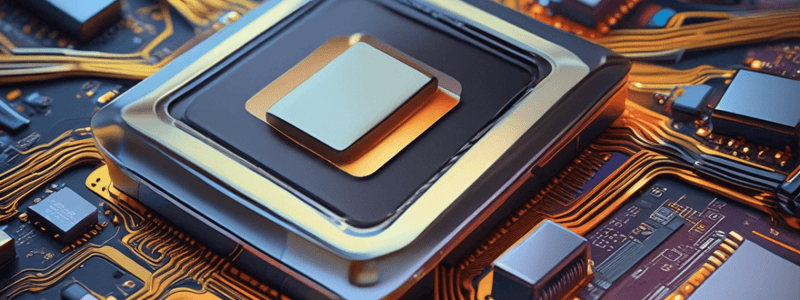
Semiconductor materials and devices play a crucial role in the technological landscape, driving advancements in diverse applications ranging from computers, smartphones, and digital cameras to medical diagnostics and environmental monitoring equipment. The key to their prominence lies in the materials themselves—semiconductors, conductors, and dielectrics—which enable technologies such as metal oxide semiconductor devices. These components offer notable features, including negligible standby power dissipation, excellent input–output isolation, surface potential control, and dependable operation.
To fully appreciate semiconductor materials and devices, we need to delve into their fundamental characteristics and the techniques used to assess their quality and reliability. This article will explore these aspects, drawing on the search results provided.
Key Components of Semiconductor Devices
Contact Resistance
Contact resistance refers to the electrical resistance between two conductors brought into contact with each other by a third conductor that can act as a source of electric charge. It is crucial for determining the effectiveness of electrical connections within devices.
Charge Pump
A charge pump is an electronic device that generates a specific output voltage from input voltages without using power amplifiers. They are used in various applications such as charging capacitors or generating high voltage signals.
Interface Quality and Oxide Trap Density
Interface quality and oxide trap density play significant roles in ensuring the reliable operation of semiconductor devices. These factors impact the overall performance and longevity of devices, making them important considerations in device design and optimization.
Techniques for Electrical Characterization of Semiconductor Materials and Devices
Current-Voltage Measurements (I-V)
Simple current-voltage measurements are used to determine basic electrical properties such as resistance, conductance, and capacitance. They provide valuable insight into the behavior of semiconductors under various conditions, helping researchers and engineers optimize device designs.
Low-Frequency Noise Analysis
Low-frequency noise analysis is a technique used to study the noise generated by electronic components at low frequencies. This information can be used to assess device reliability, detect defects, and optimize circuit designs.
Charge Pumping and Deep-Level Transient Spectroscopy (DLTS)
These advanced techniques enable detailed investigation of carrier generation, recombination processes, and defect states within semiconductor materials. By analyzing charge trapping and de-trapping phenomena, these methods help uncover crucial details about semiconductor quality and potential issues that could affect device performance.
In summary, semiconductor materials and devices have become indispensable components across numerous technological domains due to their unique characteristics and versatility. Understanding the fundamental aspects of these materials and employing precise characterization techniques are essential for pushing the boundaries of innovation in electronics, optoelectronics, and other related fields.
Studying That Suits You
Use AI to generate personalized quizzes and flashcards to suit your learning preferences.


