Podcast
Questions and Answers
What is the commonly accepted size threshold that defines nanomaterials?
What is the commonly accepted size threshold that defines nanomaterials?
- Grain sizes below 1 nm
- Grain sizes below 10 nm
- Grain sizes below 50 nm
- Grain sizes below 100 nm (correct)
Why are nanomaterials considered to have special properties?
Why are nanomaterials considered to have special properties?
- They are suitable for all applications without restrictions.
- They can be produced using any standard method.
- They are less expensive to produce.
- They have small grain sizes and unique behavior. (correct)
What happens to the special properties of nanomaterials when particles interact?
What happens to the special properties of nanomaterials when particles interact?
- They may be lost or diminished. (correct)
- They become more pronounced.
- They lead to the formation of new materials.
- They remain unchanged.
Why is the more stringent definition of nanomaterials focusing on grain sizes below 10 nm considered more useful?
Why is the more stringent definition of nanomaterials focusing on grain sizes below 10 nm considered more useful?
What is a significant characteristic of nanocrystalline ceramic materials or nanoglasses?
What is a significant characteristic of nanocrystalline ceramic materials or nanoglasses?
What occurs to the optical absorption spectra of semiconducting nanoparticles as their size decreases?
What occurs to the optical absorption spectra of semiconducting nanoparticles as their size decreases?
What is defined as the energy separation between the top filled energy level of the valence band and the nearest unfilled level in the conduction band?
What is defined as the energy separation between the top filled energy level of the valence band and the nearest unfilled level in the conduction band?
In which condition is an exciton categorized as a Mott-Wannier exciton?
In which condition is an exciton categorized as a Mott-Wannier exciton?
What happens to the band gap of Cd2P2 as the size of its particles decreases to ~15 Å?
What happens to the band gap of Cd2P2 as the size of its particles decreases to ~15 Å?
Which statement about excitons is false?
Which statement about excitons is false?
Flashcards are hidden until you start studying
Study Notes
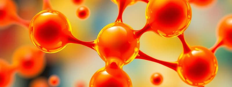
Definition of Nanomaterials
- Nanomaterials are defined as materials with grain sizes typically below 100 nm.
- A stricter definition focuses on materials with special properties due to their small grain size, often considering sizes below 10 nm.
Importance of Effective Properties
- The second definition is more critical as it highlights the necessity of special properties in nanomaterials, justifying their expense.
- Nanomaterials without unique properties are deemed impractical given their high cost.
Unique Characteristics
- Nanocrystalline ceramics and nanoglasses with particle sizes under 10 nm display notable physical properties.
- Properties related to grain boundaries differ from those of individual isolated particles.
Interaction and Special Properties
- When nanoparticles interact, their special properties may diminish.
- This interaction emphasizes the need for nanocomposites to maintain desirable characteristics.
Nanoparticles and Semiconductors
- Cadmium, germanium, and silicon nanoparticles do not exhibit semiconductor properties.
- Silicon nanoparticles can be produced through laser evaporation on a silicon substrate in a helium gas environment.
- A UV laser is used to photolyze neutral clusters, resulting in ionized clusters, which are analyzed using mass spectrophotometry.
Optical Properties of Nanoparticles
- Notable alteration in optical properties occurs in semiconducting nanoparticles compared to bulk materials.
- Optical absorption spectra shift towards the blue (shorter wavelengths) as nanoparticle size is reduced.
Excitons in Semiconductors
- Bulk semiconductors can form bound electron-hole pairs known as excitons when exposed to photons with energy exceeding the band gap.
- The band gap refers to the energy difference between the valence band's highest filled level and the conduction band's nearest unfilled level.
- Photon absorption can excite electrons from the valence band to the conduction band, creating a positive hole.
- The coulombic attraction between electron and hole results in the formation of an exciton, which affects the semiconductor's electronic and optical absorption characteristics.
Types of Excitons
- Frenkel Exciton: Formed when electron-hole separation is similar to lattice constants; tightly bound.
- Mott-Wannier Exciton: Formed when electron-hole separation significantly exceeds lattice constants; weakly bound.
Specific Material Properties
- Cd2P2 is a dark brown semiconductor with an energy gap of about 0.5 eV.
- As Cd2P2 particles decrease in size from ~30Å to ~15Å, the color transitions from brown to red, yellow, and ultimately white, with the band gap increasing to 4 eV at ~15Å.
- CdS, a bulk semiconductor, has a band gap of 2.42 eV and is orange; as particle size decreases, the energy gap increases, shifting color from yellowish to white.
Studying That Suits You
Use AI to generate personalized quizzes and flashcards to suit your learning preferences.