Podcast
Questions and Answers
What is the primary focus of Micron’s memory R&D facility in Boise?
What is the primary focus of Micron’s memory R&D facility in Boise?
- Validating advanced and unreleased memory technologies (correct)
- Creating software solutions for memory management
- Researching sustainable cleanroom construction
- Testing older memory technologies
What significant investment has Micron made in the Boise facility?
What significant investment has Micron made in the Boise facility?
- $15 billion (correct)
- $10 billion
- $20 billion
- $12 billion
Which machine is used by Micron to test and diagnose issues with silicon wafers?
Which machine is used by Micron to test and diagnose issues with silicon wafers?
- Diamond blade slicer
- EUV lithography system
- UF 3000 wafer probing machine (correct)
- Cleanroom atmospheric tester
What role do the picoprobes play in the wafer testing process?
What role do the picoprobes play in the wafer testing process?
What is the purpose of thinning the wafers in Micron's process?
What is the purpose of thinning the wafers in Micron's process?
During the encapsulation process, what is used to protect the dies?
During the encapsulation process, what is used to protect the dies?
What is the significance of the rigorous characterization testing after encapsulation?
What is the significance of the rigorous characterization testing after encapsulation?
What technology is being deployed by Micron in the development of their upcoming nodes?
What technology is being deployed by Micron in the development of their upcoming nodes?
What purpose does the specialized bending machine serve in Micron's quality testing process?
What purpose does the specialized bending machine serve in Micron's quality testing process?
Which advanced diagnostic tool allows engineers to inspect dies at the gate and transistor level?
Which advanced diagnostic tool allows engineers to inspect dies at the gate and transistor level?
What type of testing do the servers in Micron's Long-Term Burn-In and Validation Lab perform?
What type of testing do the servers in Micron's Long-Term Burn-In and Validation Lab perform?
What is a key feature of Micron's multi-stage automated PCV production line?
What is a key feature of Micron's multi-stage automated PCV production line?
What type of modules undergo testing using a CNC cutter?
What type of modules undergo testing using a CNC cutter?
Why is the Micron R&D facility described as having a 'secret' regarding certain modules?
Why is the Micron R&D facility described as having a 'secret' regarding certain modules?
What does the EMI test chamber at Micron measure?
What does the EMI test chamber at Micron measure?
What is the significance of using only prime-quality dies in Micron's consumer Crucial branded DIMMs?
What is the significance of using only prime-quality dies in Micron's consumer Crucial branded DIMMs?
How does Micron handle defectively screened memory modules?
How does Micron handle defectively screened memory modules?
Flashcards
Wafer Probing
Wafer Probing
Using tiny probes to test and analyze individual dies on a silicon wafer.
Wafer Thinning
Wafer Thinning
Reducing the thickness of a wafer using specialized machines to improve handling precision, and enabling better access to components from both sides of the wafer.
Wafer Slicing
Wafer Slicing
Cutting the thinned wafer to separate individual dies, using extremely thin diamond blades.
Die Encapsulation
Die Encapsulation
Signup and view all the flashcards
DDR5 Memory Module
DDR5 Memory Module
Signup and view all the flashcards
EUV Lithography
EUV Lithography
Signup and view all the flashcards
Picoprobes
Picoprobes
Signup and view all the flashcards
Cleanroom Environment
Cleanroom Environment
Signup and view all the flashcards
Automated PCV Production Line
Automated PCV Production Line
Signup and view all the flashcards
Quality Control System (Micron)
Quality Control System (Micron)
Signup and view all the flashcards
Memory Module Bending Tests
Memory Module Bending Tests
Signup and view all the flashcards
X-ray Machine Testing
X-ray Machine Testing
Signup and view all the flashcards
Scanning Electron Microscope Testing
Scanning Electron Microscope Testing
Signup and view all the flashcards
Heating/Cooling Cycle
Heating/Cooling Cycle
Signup and view all the flashcards
CNC Cutter Testing
CNC Cutter Testing
Signup and view all the flashcards
Long-Term Burn-In
Long-Term Burn-In
Signup and view all the flashcards
EMI Test Chamber
EMI Test Chamber
Signup and view all the flashcards
R&D Facility Location
R&D Facility Location
Signup and view all the flashcards
Study Notes
Micron's Memory R&D Center of Excellence in Boise
-
Micron’s memory research and development facility in Boise, Idaho, is a cutting-edge center for silicon development, fabrication, and testing.
-
The facility houses over 200,000 square feet of dedicated space, featuring a Class 100 cleanroom environment.
-
Micron has invested $15 billion in expanding the facility, with plans to add 600,000 square feet of sustainable cleanroom manufacturing space by 2025.
-
This facility focuses on researching and validating new memory technologies, with an emphasis on advanced, unreleased technologies.
-
Micron is currently deploying EUV lithography systems as part of the development of their upcoming 1-gamma and 1-delta nodes.
-
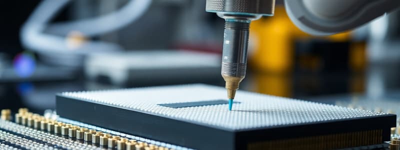
Micron uses a UF 3000 wafer probing machine to test and diagnose issues with new silicon wafers.
-
This machine allows engineers to probe individual dies with high precision through a combination of machine vision and manual input.
Wafer Probing and Characterization
-
Micron utilizes picoprobes, which are incredibly tiny and precise tools, to test and analyze the internal functionality of dies.
-
The picoprobes allow engineers to perform detailed investigations into the inner workings of the dies, revealing insights that traditional probes cannot achieve.
-
To maximize the testing and analysis of wafers, they are often cut in half, enabling multiple engineers to inspect and diagnose issues simultaneously.
Wafer Thinning and Slicing
-
Thinning the wafer is a crucial step in the process. Micron uses a specialized machine to thin the wafers, applying a plastic protective film and then grinding the wafer down to a specific thickness.
-
The thinned wafers are then sliced using diamond blades that are incredibly thin, akin to the width of a human finger hair.
-
This process allows for precise cutting of individual dies while adhering to the sticky backing material.
Encapsulation and Packaging
-
Encapsulation involves packaging the dies, which involves stacking multiple dies, bonding them with exceptional precision, and attaching bond wires to facilitate soldering onto a board.
-
The encapsulated dies are then embedded within an epoxy or a mold compound to protect them during transportation and use.
DDR5 Memory Module Production
-
After encapsulation, the dies undergo rigorous characterization testing, which verifies their functionality.
-
These tests are essential to ensure that the dies perform adequately at high speeds, meeting the demanding requirements of Micron's customers.
-
Micron utilizes a multi-stage automated PCV production line for the production of memory modules.
-
The line includes robots for pick-and-place operations, silk screening of solder paste, and various testing and inspection stages.
-
Defectively screened memory modules can undergo a manual repair process, where errors can be corrected before the next stage.
Quality Testing and Characterization
-
Micron uses a specialized bending machine to assess the performance of packaged modules.
-
This machine simulates various environmental conditions, including hot and cold temperatures, to test the modules' durability and resilience.
-
The bending machine helps determine the variation in module performance and identify any potential problems that may arise.
-
Micron implements a multi-level quality control system to ensure the production of high-quality memory modules, with only prime-quality dies being used in their consumer Crucial branded DIMMs.
Advanced Diagnostic Tools
-
X-ray machines are used to non-destructively diagnose potential issues in individual dies or modules.
-
Scanning electron microscopes offer an even higher level of detail, allowing engineers to scrutinize the dies at the gate and transistor level, further assisting in problem diagnosis.
-
Micron's R&D facility employs a comprehensive range of advanced testing and diagnostic tools to ensure the development and production of cutting-edge memory technologies.
Memory Module Testing
- Memory modules go through a heating cycle (heating, holding, cooling) before being tested
- Modules are prepped with components on one side and tested on the other
- Modules are tested using a CNC cutter
- The CNC has a safety check to ensure the correct gripper is loaded for the type of module (SODIMMs, DIMMs, DDR4, DDR5)
Long-Term Burn-In and Validation Lab
- Micron has servers that test new memory modules for thousands of hours
- Tests are conducted on consumer motherboards
- They hold validation boards for various platforms to test customer complaints
- Micron works with a range of companies, including automotive manufacturers, dishwasher manufacturers, etc. to test memory
- Micron has a large EMI test chamber that measures radio emissions from modules to ensure regulatory compliance and limit unwanted radiation
Module Testing
- Micron's testing labs are often equipped with unreleased hardware, making public filming difficult.
- The modules are tested in a test bench
- The 24 Gigabyte modules are a "secret" and are not for sale, and the Micron representative is not allowed to provide more detail.
Micron R&D Facility
- Micron R&D is based in Idaho, USA.
- It is the largest R&D facility for storage and memory products in the Western Hemisphere.
- It has a large number of electrical panels and testing equipment.
- The facility houses 50,000 patents related to storage and memory technologies.
- There are "secret" 24 GB modules that were not supposed to leave the lab.
Studying That Suits You
Use AI to generate personalized quizzes and flashcards to suit your learning preferences.


