Podcast
Questions and Answers
What is a primary function of the base material in a printed circuit board (PCB)?
What is a primary function of the base material in a printed circuit board (PCB)?
- It increases the weight of the PCB for stability.
- It conducts electricity to power the components.
- It facilitates heat dissipation from the components.
- It acts as an insulating layer to prevent electrical conduction. (correct)
Which material is most commonly used as a dielectric in PCBs?
Which material is most commonly used as a dielectric in PCBs?
- FR-4 (correct)
- Phenolic resin
- Polyethylene
- Polypropylene
What criteria must the base layer of a PCB satisfy?
What criteria must the base layer of a PCB satisfy?
- It should be able to withstand high temperatures. (correct)
- It should be a good conductor of electricity.
- It should enhance the signal transmission speed.
- It must be lightweight to reduce costs.
What is the primary purpose of a via in a double-sided PCB?
What is the primary purpose of a via in a double-sided PCB?
Which statement about dielectric loss in PCB materials is true?
Which statement about dielectric loss in PCB materials is true?
What issue can arise from poor quality base materials in a PCB?
What issue can arise from poor quality base materials in a PCB?
Which characteristic of double-sided PCBs enhances their suitability for complex circuits?
Which characteristic of double-sided PCBs enhances their suitability for complex circuits?
Which of the following is NOT a characteristic of a dielectric material used in PCBs?
Which of the following is NOT a characteristic of a dielectric material used in PCBs?
What is typically found in a multi-layer PCB design?
What is typically found in a multi-layer PCB design?
In the PCB manufacturing process, what is usually the first step after component layout?
In the PCB manufacturing process, what is usually the first step after component layout?
What is the purpose of laminates and prepregs in PCB construction?
What is the purpose of laminates and prepregs in PCB construction?
Which type of dielectric layer is typically not used in PCB applications?
Which type of dielectric layer is typically not used in PCB applications?
What aspect of multi-layer PCBs makes them essential for implementing complex circuits?
What aspect of multi-layer PCBs makes them essential for implementing complex circuits?
What method is commonly used to design the circuit track for a PCB?
What method is commonly used to design the circuit track for a PCB?
How does the construction of double-sided PCBs differ from single-sided boards?
How does the construction of double-sided PCBs differ from single-sided boards?
Why are breadboards often used during the initial layout phase of PCB design?
Why are breadboards often used during the initial layout phase of PCB design?
What is the main function of the ground plane in a multi-layer PCB?
What is the main function of the ground plane in a multi-layer PCB?
Which of the following describes creepage in the context of PCB design?
Which of the following describes creepage in the context of PCB design?
Why are multi-layer PCBs typically more expensive to manufacture than single- or double-sided boards?
Why are multi-layer PCBs typically more expensive to manufacture than single- or double-sided boards?
What is the primary benefit of using a multi-layer PCB?
What is the primary benefit of using a multi-layer PCB?
In a multi-layer PCB, why is it recommended to dedicate one complete layer to a ground plane?
In a multi-layer PCB, why is it recommended to dedicate one complete layer to a ground plane?
Which type of via in PCB design connects the outer surface to an inner layer only?
Which type of via in PCB design connects the outer surface to an inner layer only?
What happens when a PCB designer moves from a 4-layer to a 6-layer design?
What happens when a PCB designer moves from a 4-layer to a 6-layer design?
Which layer configuration is most common for multi-layer PCBs?
Which layer configuration is most common for multi-layer PCBs?
What is the consequence of using too tight a clearance between tracks and pads on a PCB?
What is the consequence of using too tight a clearance between tracks and pads on a PCB?
Which of the following track width dimensions is considered adequate for signal tracks at a minimum?
Which of the following track width dimensions is considered adequate for signal tracks at a minimum?
What factor significantly influences the resistance of a PCB track?
What factor significantly influences the resistance of a PCB track?
For basic through-hole designs, what is a recommended minimum clearance limit?
For basic through-hole designs, what is a recommended minimum clearance limit?
What characteristic of tracks does a lower track/space figure indicate?
What characteristic of tracks does a lower track/space figure indicate?
Why is it common practice for designers to use wider tracks initially?
Why is it common practice for designers to use wider tracks initially?
What is the standard lower limit for spacing between tracks in a typical PCB design?
What is the standard lower limit for spacing between tracks in a typical PCB design?
What track width may some designers prefer for aesthetic reasons?
What track width may some designers prefer for aesthetic reasons?
What is the primary function of a through-hole in a PCB?
What is the primary function of a through-hole in a PCB?
Which statement best describes the difference between a via and a through-hole?
Which statement best describes the difference between a via and a through-hole?
Which side of a single-sided PCB is referred to as the 'solder side'?
Which side of a single-sided PCB is referred to as the 'solder side'?
What is a primary advantage of Surface Mounted Technology (SMT) over Through-Hole Technology (THT)?
What is a primary advantage of Surface Mounted Technology (SMT) over Through-Hole Technology (THT)?
When is a landless via used?
When is a landless via used?
Which feature of SMT makes it challenging for manual assembly?
Which feature of SMT makes it challenging for manual assembly?
What is the effect of increasing track width in PCB design?
What is the effect of increasing track width in PCB design?
How do surface-mounted components differ from traditional through-hole components in terms of PCB design?
How do surface-mounted components differ from traditional through-hole components in terms of PCB design?
Why are vias typically smaller in diameter compared to through-holes?
Why are vias typically smaller in diameter compared to through-holes?
What characteristic is necessary for solder to adhere properly to a through-hole?
What characteristic is necessary for solder to adhere properly to a through-hole?
Which of the following describes the function of edge connectors in PCB terminology?
Which of the following describes the function of edge connectors in PCB terminology?
What typically happens in a PCB design strictly using surface mount devices?
What typically happens in a PCB design strictly using surface mount devices?
What is a key difference between the legs of SMT components and THT components?
What is a key difference between the legs of SMT components and THT components?
Which of the following is true regarding the ratio of pad size to hole size in PCB design?
Which of the following is true regarding the ratio of pad size to hole size in PCB design?
What does a heat sink do in PCB terminology?
What does a heat sink do in PCB terminology?
Which statement is true about the comparative costs of SMT and THT components?
Which statement is true about the comparative costs of SMT and THT components?
Flashcards
Component Side of PCB
Component Side of PCB
The side of a single-sided PCB where components are placed.
Solder Side of PCB
Solder Side of PCB
The opposite side of a single-sided PCB where the solder connections are made.
SMT (Surface Mount Technology)
SMT (Surface Mount Technology)
A method of placing electronic components directly onto a circuit board.
SMT component size
SMT component size
Signup and view all the flashcards
SMT component soldering
SMT component soldering
Signup and view all the flashcards
PCB Foil Pattern
PCB Foil Pattern
Signup and view all the flashcards
Heat Sinks
Heat Sinks
Signup and view all the flashcards
Edge Connectors
Edge Connectors
Signup and view all the flashcards
What are vias?
What are vias?
Signup and view all the flashcards
What's the benefit of double-sided PCBs?
What's the benefit of double-sided PCBs?
Signup and view all the flashcards
Multi-layer PCBs
Multi-layer PCBs
Signup and view all the flashcards
What's the basic process of PCB manufacture?
What's the basic process of PCB manufacture?
Signup and view all the flashcards
Why are components laid out on a breadboard?
Why are components laid out on a breadboard?
Signup and view all the flashcards
What's the purpose of PCB creation software?
What's the purpose of PCB creation software?
Signup and view all the flashcards
Why is circuit track design done with software?
Why is circuit track design done with software?
Signup and view all the flashcards
What is the purpose of component layout on a PCB?
What is the purpose of component layout on a PCB?
Signup and view all the flashcards
PCB Manufacturing Process
PCB Manufacturing Process
Signup and view all the flashcards
PCB Substrate
PCB Substrate
Signup and view all the flashcards
Dielectric Material
Dielectric Material
Signup and view all the flashcards
FR-4
FR-4
Signup and view all the flashcards
Laminate vs. Prepreg
Laminate vs. Prepreg
Signup and view all the flashcards
Why is a PCB Substrate Non-Conductive?
Why is a PCB Substrate Non-Conductive?
Signup and view all the flashcards
Open Circuit
Open Circuit
Signup and view all the flashcards
Delamination
Delamination
Signup and view all the flashcards
What's the difference between a via and a through-hole?
What's the difference between a via and a through-hole?
Signup and view all the flashcards
Blind Via
Blind Via
Signup and view all the flashcards
Landless Via
Landless Via
Signup and view all the flashcards
What are the benefits of larger track width?
What are the benefits of larger track width?
Signup and view all the flashcards
What is the purpose of the copper area around a through-hole?
What is the purpose of the copper area around a through-hole?
Signup and view all the flashcards
Why are vias typically smaller than through-holes?
Why are vias typically smaller than through-holes?
Signup and view all the flashcards
Why are surface-mounted devices preferred over through-hole components?
Why are surface-mounted devices preferred over through-hole components?
Signup and view all the flashcards
Track/Space Resolution
Track/Space Resolution
Signup and view all the flashcards
Track Width
Track Width
Signup and view all the flashcards
Clearance
Clearance
Signup and view all the flashcards
Track Thickness
Track Thickness
Signup and view all the flashcards
Solder Coating Finish
Solder Coating Finish
Signup and view all the flashcards
PCB Manufacturing Cost
PCB Manufacturing Cost
Signup and view all the flashcards
Electrical Clearances for SMT
Electrical Clearances for SMT
Signup and view all the flashcards
Design for Manufacturability (DFM)
Design for Manufacturability (DFM)
Signup and view all the flashcards
PCB Clearance vs. Creepage
PCB Clearance vs. Creepage
Signup and view all the flashcards
Why Multi-Layer PCBs are Used
Why Multi-Layer PCBs are Used
Signup and view all the flashcards
Common Multi-Layer PCB Configurations
Common Multi-Layer PCB Configurations
Signup and view all the flashcards
Dedicated Layers in Multi-Layer PCBs
Dedicated Layers in Multi-Layer PCBs
Signup and view all the flashcards
Types of Vias in Multi-Layer PCBs
Types of Vias in Multi-Layer PCBs
Signup and view all the flashcards
Why Use More Multi-Layer PCBs?
Why Use More Multi-Layer PCBs?
Signup and view all the flashcards
Multi-Layer PCB Advantages
Multi-Layer PCB Advantages
Signup and view all the flashcards
Study Notes
Printed Circuit Boards (PCBs)
- PCBs are flat, insulating surfaces. Wiring and components are connected on a predetermined design.
- Components are attached to a common base.
- PCBs are used to reduce the overall size of electronic equipment.
Introduction to PCBs
- PCBs are flat insulating surfaces with printed wiring and miniature components.
- They are in a predetermined design and attached to a common base.
- Components are connected on the board and wiring is on the reverse.
Preceding Technology
- Before PCBs, circuits were constructed laboriously with point-to-point wiring.
- This led to frequent failures, short circuits, and problems with aging, cracking wire insulation.
- PCBs are now in almost every electronic device, big or small.
- PCBs provide electrical connections between mounted components.
- Device complexity leads to more densely populated PCBs.
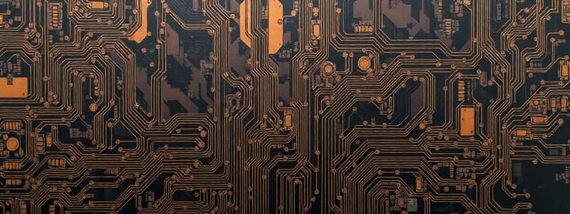
Basic PCB Construction
- PCBs are made from various materials; often a flat laminated composite.
- Materials are non-conductive substrate materials with layers of copper circuit, generally inside or on the surface.
- The flat composite supports components, while copper conductors connect them.
- PCBs can be single- or double-layered, or have numerous layers in more complex applications.
Base or Substrate Materials
- PCBs use phenolic paper, epoxy paper, or epoxy glass as their base.
- Cladding is typically copper, but other metals are possible.
- The substrate, or laminate, is produced first, followed by bonding the cladding.
Conductor Patterns
- The substrate is a non-flexible, insulating material. Copper foil etched away becomes conductor patterns (tracks) on the board surface.
- These tracks connect components.
- A basic PCB has a copper circuit pattern on one side.
- Components (leads) are pushed through drilled holes, then soldered.
Solder Mask and Silk Screen
- The solder mask (often green or brown) is an insulating protective coating that prevents solder from attaching outside connection points.
- A silk screen (often white) with text and symbols labels component locations.
Through-Hole Technology (THT)
- Components are connected to one side and soldered on the opposite side.
- PCB holes for component legs to penetrate.
THT Component Mounting
- Components' legs are soldered to the conductor pattern.
- Basic single-sided boards have components on one side and the conductor pattern on the other.
Surface-Mounted Technology (SMT)
- Components' legs are soldered to the conductor pattern on the same side as the component is mounted.
- SMT components are smaller than THT components, more dense, and cheaper.
- SMT components are usually mounted using automated machines.
PCB Terminology
- Heat sinks: Used for dissipating heat from components.
- Voltage and ground lines: Pathways for power distribution.
- Terminals/pads: Holes to accommodate component leads.
- Conductors/runs: Foil strips between components.
- Edge connectors: Used to connect the PCB to another device.
PCB Additional Components
- Component sockets: Allow components to be removed without soldering.
Edge Connectors
- Used to connect the PCB to other devices. Small uncovered copper pads on the side of the PCB.
PCB Types
- Single-sided boards: Conductor pattern on one side. Limited for routing.
- Double-sided boards: Conductor pattern on both sides, allowing more complex circuits and routing.
- Multi-layer boards: Multiple layers of conductors and insulators. More sophisticated and complex.
Advanced PCB Construction
- PCB Manufacturing Steps: components laid out, circuit track design, and then sent for manufacturing. Components are soldered.
- High speed NiCd charger PCB Example: steps of making a PCB, starting with components laid out, then circuit track designed, and finally manufacturing.
PCB Substrate
- The base, or substrate, materials are typically phenolic paper, epoxy paper, or epoxy glass.
Dielectric
- Dielectric layers are insulating in PCB construction. Made of materials like Porcelain, mica, glass and plastics.
Copper Foil
- Copper foil is the conductor material in PCBs. Weight/thickness measures are important, 0.5 oz, 1 oz, or 2 oz.
Pads
- Pads are copper surfaces where components' legs are soldered,
- Pad sizes, shapes, and dimensions depend on components and manufacturing process.
Vias and Through-Holes
- Vias and through-holes are structures used to connect copper layers.
- Through-holes are larger and connect layers of a PCB, whereas a Via allows pin of a component to go through from one side of the board to the other.
- Vias are typically smaller than through-holes.
Tracking
- Track width depends on the manufacturer's capability of the PCB.
- Wider tracks have lower resistance.
Clearances
- Electrical clearances are crucial for prevention of shorts.
Multi-Layer Design
- Mulit-layer PCBs are typically more expensive and difficult to manufacture but offer greater density for routing and compact design. Includes layers of conductors and insulators.
Grounding
- Grounding is essential for proper circuit functionality.
Bypassing
- Bypassing uses capacitors for smoothing out power rails.
- Capacitors are placed close to the components they serve.
Flexible PCB
- Flexible PCBs have conductive layers on a flexible plastic substrate, used in applications requiring flexibility.
Studying That Suits You
Use AI to generate personalized quizzes and flashcards to suit your learning preferences.

